SLVSCQ5A December 2014 – February 2015 TPS62184
PRODUCTION DATA.
- 1 Features
- 2 Applications
- 3 Description
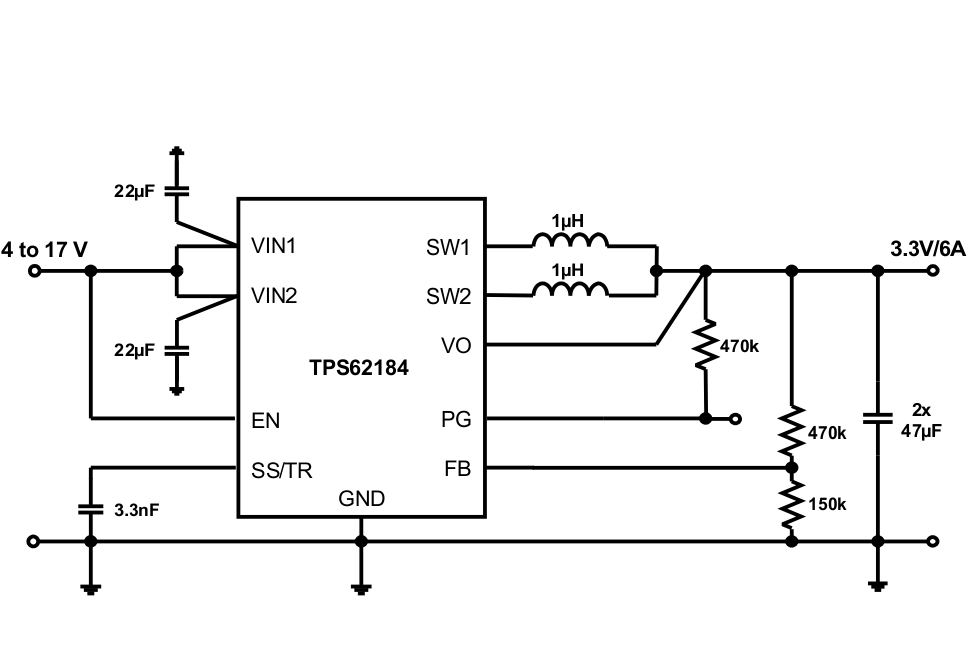
- 4 Simplified Schematic
- 5 Revision History
- 6 Pin Configuration and Functions
- 7 Specifications
- 8 Detailed Description
- 9 Application and Implementation
- 10Power Supply Recommendations
- 11Layout
- 12Device and Documentation Support
- 13Mechanical, Packaging, and Orderable Information
Package Options
Mechanical Data (Package|Pins)
- YZF|24
Thermal pad, mechanical data (Package|Pins)
Orderable Information
1 Features
- Dual Phase Balanced Peak Current Mode
- Input Voltage Range: 4 V to 17 V
- Output Voltage:
- 0.9 V ≤ VOUT ≤ 1.8 V (6A),
- 1.8 V ≤ VOUT ≤ 2.5 V (5.5A)
- 2.5 V ≤ VOUT ≤ 3.5 V (5A)
- Typical Quiescent Current of 28 µA
- Output Voltage Accuracy of ±1% (PWM Mode)
- Automatic Efficiency Enhancement (AEE™)
- Phase Shifted Operation
- Automatic Power Save Mode
- Adjustable Soft Start
- Power Good Output
- Undervoltage Lockout
- HICCUP Over Current Protection
- Over Temperature Protection
- Pin to Pin Compatible with TPS62180/2
- NanoFree™ 2.10 mm x 3.10 mm DSBGA Package
2 Applications
- Low Profile POL Supply
- NVDC Powered Systems
- Dual/Triple Cell Li-ion Battery
- Ultra Portable/Embedded/Tablet PC
- Computing Network Solutions
- Micro Server, SSD
3 Description
The TPS62184 is a synchronous dual-phase step-down DC-DC converter for low profile power rails. It operates with two identical, current balanced phases that are peak current controlled enabling use in height limited applications.
With a wide operating input voltage range of 4 V to 17 V, the device is ideally suited for systems powered from multi-cell Li-Ion batteries or 12-V rails. The output current of 6 A is continuously provided by two phases of 3 A each, allowing the use of low profile external components. The phases operate out of phase, reducing switching noise significantly.
The TPS62184 automatically enters Power Save Mode to maintain high efficiency down to very light loads. It also incorporates an Automatic Efficiency Enhancement (AEETM) for the entire duty cycle range.
The device features a Power Good signal, as well as an adjustable soft start. The quiescent current is typically 28 µA, it is able to run in 100% mode, and it has no duty cycle limitation even at lowest output voltage.
The TPS62184 is packaged in a small 24-bump, 0.5 mm pitch DSBGA package.
Device Information(1)
| PART NUMBER | PACKAGE | BODY SIZE (NOM) |
|---|---|---|
| TPS62184 | DSBGA (24) | 2.10 mm x 3.10 mm |
- For all available packages, see the orderable addendum at the end of the datasheet.
4 Simplified Schematic

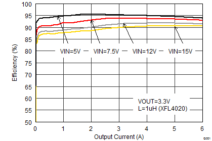
Efficiency vs Output Current
