SLVSBO3A December 2013 – December 2015 TPS657120
PRODUCTION DATA.
- 1 Device Overview
- 2 Revision History
- 3 Terminal Configuration and Functions
-
4 Specifications
- 4.1 Absolute Maximum Ratings
- 4.2 ESD Ratings
- 4.3 Recommended Operating Conditions
- 4.4 Thermal Information
- 4.5 Electrical Characteristics: General Functions
- 4.6 Electrical Characteristics: DCDC1 and DCDC2
- 4.7 Electrical Characteristics: DCDC3
- 4.8 Electrical Characteristics: RF-LDOs
- 4.9 Electrical Characteristics: Digital Inputs, Digital Outputs
- 4.10 Electrical Characteristics: Thermal Shutdown, Undervoltage Lockout
- 4.11 Electrical Characteristics: RFFE Timing Parameters
- 4.12 Typical Characteristics
-
5 Detailed Description
- 5.1 Overview
- 5.2 Functional Block Diagram
- 5.3
Feature Description
- 5.3.1 Default Settings
- 5.3.2 Linear Regulators
- 5.3.3 Step-down Converters DCDC1 and DCDC2
- 5.3.4 Power Save Mode
- 5.3.5 Dynamic Voltage Positioning (Optional)
- 5.3.6 Soft Start / Enable
- 5.3.7 Dynamic Voltage Scaling (DVS) for DCDC1, DCDC2 and DCDC3
- 5.3.8 100% Duty Cycle Low Dropout Operation
- 5.3.9 180° Out-of-Phase Operation
- 5.3.10 Undervoltage Lockout for DCDC1, DCDC2, DCDC3, LDO1 and LDO2
- 5.3.11 Output Voltage Discharge
- 5.3.12 Short-Circuit Protection
- 5.3.13 Output Voltage Monitoring
- 5.3.14 Step-Down Converter and LDO Enable; pins CLK_REQ1 and CLK_REQ2
- 5.3.15 Step-Down Converter DCDC3
- 5.3.16 DCDC3_SEL Control
- 5.3.17 Bypass Switch
- 5.3.18 DCDC3 Output Voltage Ramp Support
- 5.3.19 VCON Decoder
- 5.3.20 Thermal Monitoring and Shutdown
- 5.3.21 GPIOs
- 5.3.22 nRESET Input ; ADR_SELECT Input
- 5.3.23 Power State Machine
- 5.3.24 Implementation of Internal Power-Up and Power-Down Sequencing
- 5.3.25 VDDIO Voltage for Push-pull Output Stages / Interface
- 5.3.26 TPS657120 On Off Operation
- 5.3.27 MIPI RFFE Interface
- 5.4 Device Functional Modes
- 5.5 Register Maps
- 6 Application and Implementation
- 7 Power Supply Recommendations
- 8 Layout
- 9 Device and Documentation Support
- 10Mechanical, Packaging, and Orderable Information
Package Options
Mechanical Data (Package|Pins)
- YFF|30
Thermal pad, mechanical data (Package|Pins)
Orderable Information
1 Device Overview
1.1 Features
- 3 Step-Down Converters:
- 2 LDOs:
- 2 × 10-mA Output Current
- Low Noise RF-LDOs
- Output Voltage Range 1.2 V to 3.4 V
- 32-μA Quiescent Current
- Pre-Regulation Support by Separate Power Inputs
- ECO mode
- VIN Range of LDOs:
- LDO1: 2.0 V to 5.5 V
- LDO2: 2.8 V to 5.5 V
- 2 GPIOs
- Thermal Shutdown
- Bypass Switch
- Used with DCDC3 Powering an RF-PA
- Interface
- 26 MHz-MIPI RFFE Interface
- Undervoltage Lockout
- Flexible Power-Up and Power-Down Sequencing
- 2.5-mm × 2.3-mm DSBGA Package with 0.4-mm Pitch
1.2 Applications
- Data Cards
- Smartphones
1.3 Description
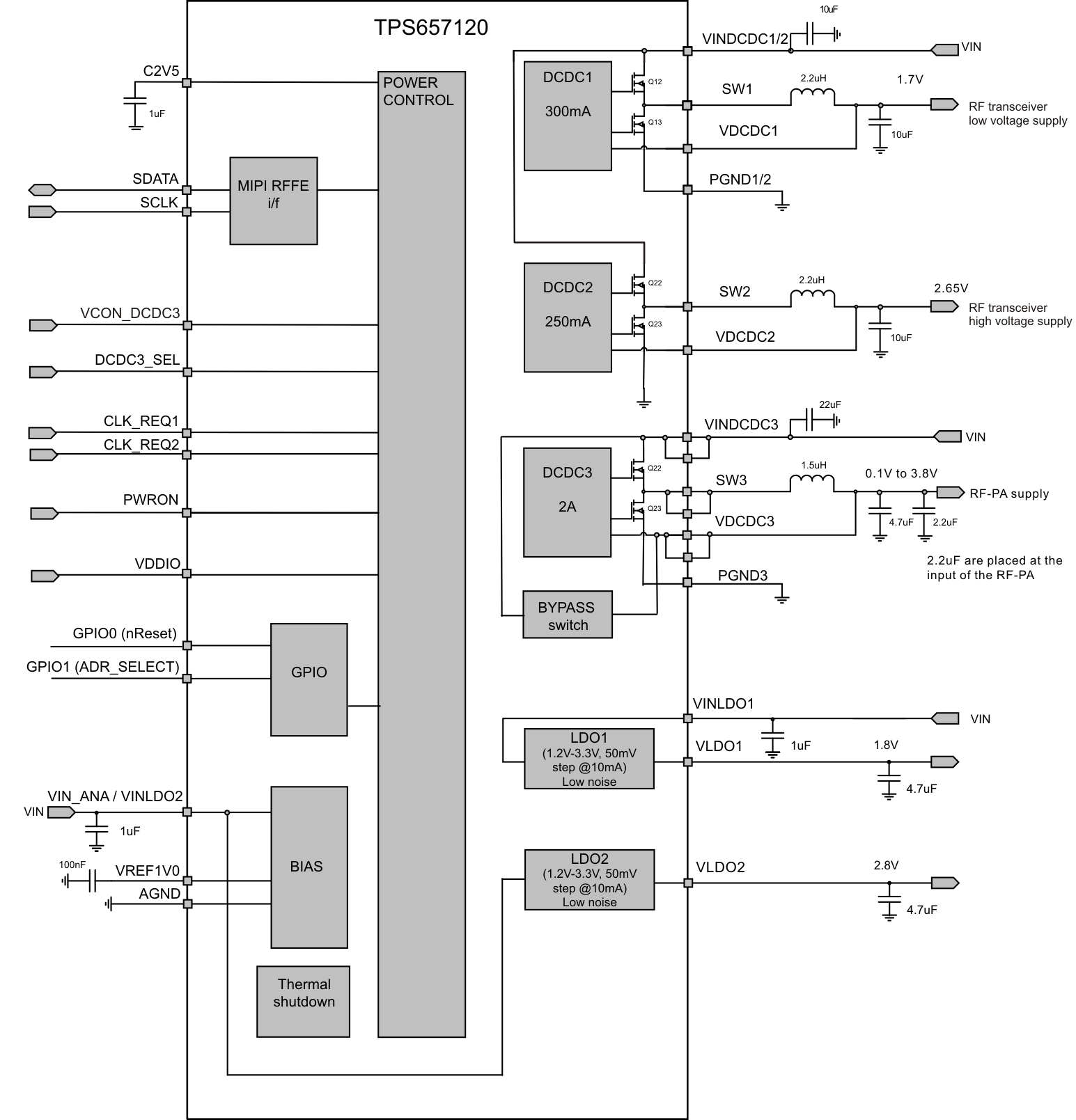
The TPS657120 provides three configurable step-down converters with up to 2-A output current.This device also has 2 LDO regulators. LDO1 can be supplied from either the input voltage directly or from a pre-regulated supply such as DCDC1 or DCDC2. The input voltage to LDO2 is used as an analog supply input and therefore must be tied to the input voltage at the same voltage level with VINDCDC1/2 and VINDCDC3. The internal power-up and power-down controller is configurable and can support any power-up/power-down sequences (OTP based). All LDOs and DCDC converters are controllable by a MIPI RFFE compatible interface, by pins PWRON, CLK_REQ1 and CLK_REQ2, or both. In addition, there is a nRESET as well as a RFFE address select (ADR_SELECT) input which can alternatively be used as general purpose I/Os with a 1-mA sink capability. The TPS657120 comes in a 6-ball × 5-ball DSBGA package (2.5 mm × 2.3 mm) with a 0.4-mm pitch.
Device Information(1)
| PART NUMBER | PACKAGE | BODY SIZE (NOM) |
|---|---|---|
| TPS657120 | DSBGA (30) | 2.31 mm × 2.51 mm |
1.4 Functional Block Diagram
 Figure 1-1 Functional Block Diagram