SLVSCJ8B November 2014 – January 2015
PRODUCTION DATA.
- 1 Features
- 2 Applications
- 3 Description
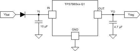
- 4 Typical Application Schematic
- 5 Revision History
- 6 Pin Configuration and Functions
- 7 Specifications
- 8 Detailed Description
- 9 Application and Implementation
- 10Power Supply Recommendations
- 11Layout
- 12Device and Documentation Support
- 13Mechanical, Packaging, and Orderable Information
Package Options
Mechanical Data (Package|Pins)
Thermal pad, mechanical data (Package|Pins)
- DCY|4
Orderable Information
1 Features
- Qualified for Automotive Applications
- AEC-Q100 Qualified With the Following Results:
- Device Temperature Grade 1: –40°C to 125°C Ambient Operating Temperature Range
- Device HBM ESD Classification Level 2
- Device CDM ESD Classification Level C4B
- 4 to 40-V Wide VI Input Voltage Range With up to 45-V Transient
- Maximum Output Current: 150 mA
- Low Quiescent Current (IQ):
- 15 µA Typical at Light Loads
- 25 µA Maximum Under Full Temperature
- 450-mV Typical Low Dropout Voltage at 100 mA Load Current
- Stable With Low ESR Ceramic Output Capacitor (2.2 to 100 µF)
- Fixed 2.5-V, 3.3-V, and 5-V Output Voltage Options
- Integrated Fault Protection:
- Thermal Shutdown
- Short-Circuit Protection
- Packages:
- 4-Pin SOT-223 Package
- 5-Pin SOT-23 Package
2 Applications
- Automotive
- Infotainment Systems With Sleep Mode
- Always-On Battery Applications
- Door Modules
- Remote Keyless-Entry Systems
- Immobilizers
3 Description
The TPS7B69xx-Q1 device is a low-dropout linear regulator designed for up to 40-V VI operations. With only 15-µA (typical) quiescent current at light load, the device is suitable for standby microcontrol-unit systems especially in automotive applications.
The devices feature an integrated short-circuit and overcurrent protection. The TPS7B69xx-Q1 device operates over a –40°C to 125°C temperature range. Because of these features, the TPS7B6925-Q1, TPS7B6933-Q1, and TPS7B6950-Q1 devices are well suited in power supplies for various automotive applications.
Device Information(1)
| PART NUMBER | PACKAGE | BODY SIZE (NOM) |
|---|---|---|
| TPS7B6925-Q1 TPS7B6933-Q1 TPS7B6950-Q1 |
SOT-223 (4) | 6.50 mm × 3.50 mm |
| SOT-23 (5) | 2.90 mm × 1.60 mm |
- For all available packages, see the orderable addendum at the end of the datasheet.
4 Typical Application Schematic