SGLS318A November 2005 – November 2015 UC2854B-EP
PRODUCTION DATA.
- 1 Features
- 2 Applications
- 3 Description
- 4 Revision History
- 5 Description (continued)
- 6 Pin Configuration and Functions
- 7 Specifications
- 8 Detailed Description
-
9 Application and Implementation
- 9.1 Application Information
- 9.2
Typical Application
- 9.2.1 Design Requirements
- 9.2.2
Detailed Design Procedure
- 9.2.2.1 Switching Frequency
- 9.2.2.2 Inductor Selection
- 9.2.2.3 Output Capacitor
- 9.2.2.4 Switch and Diode
- 9.2.2.5 Current Sensing
- 9.2.2.6 Peak Current Limit
- 9.2.2.7 Multiplier Set-up
- 9.2.2.8 Feedforward Voltage
- 9.2.2.9 Multiplier Input Current
- 9.2.2.10 Oscillator Frequency
- 9.2.2.11 Current Error Amplifier Compensation
- 9.2.2.12 Voltage Error Amplifier Compensation
- 9.2.2.13 Feedforward Voltage Divider Filter Capacitors
- 9.2.2.14 Design Procedure Summary
- 9.2.3 Application Curve
- 10Power Supply Recommendations
- 11Layout
- 12Device and Documentation Support
- 13Mechanical, Packaging, and Orderable Information
Package Options
Mechanical Data (Package|Pins)
- DW|16
Thermal pad, mechanical data (Package|Pins)
- DW|16
Orderable Information
1 Features
- Controlled Baseline
- One Assembly/Test Site, One Fabrication Site
- Extended Temperature Performance of −55°C to 125°C
- Enhanced Diminishing Manufacturing Sources (DMS) Support
- Enhanced Product-Change Notification
- Qualification Pedigree (1)
- Controls Boost PWM to Near-Unity Power Factor
- Limits Line Current Distortion to <3%
- World-Wide Operation Without Switches
- Accurate Power Limiting
- Fixed-Frequency Average Current-Mode Control
- High Bandwidth (5 MHz), Low-Offset Current Amplifier
- Integrated Current- and Voltage Amplifier Output Clamps
- Multiplier Improvements: Linearity, 500 mV VAC Offset (Eliminates External Resistor), 0 V to 5 V Multout Common-Mode Range
- VREF GOOD Comparator
- Faster and Improved Accuracy ENABLE Comparator
- UVLO Options (16 V/10 V or 10.5 V/10 V)
- 300-μA Start-Up Supply Current
2 Applications
Industrial Lighting
3 Description
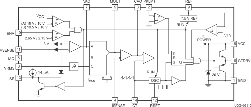
The UC2854B products are pin compatible enhanced versions of the UC2854. Like the UC2854, these products provide all of the functions necessary for active power factor corrected preregulators. The controller achieves near unity power factor by shaping the ac-input line current waveform to correspond to the ac-input line voltage. To do this the UC2854B uses average current mode control. Average current mode control maintains stable, low distortion sinusoidal line current without the need for slope compensation, unlike peak current mode control.
A 1% 7.5-V reference, fixed frequency oscillator, PWM, voltage amplifier with soft-start, line voltage feedforward (VRMS squarer), input supply voltage clamp, and over current comparator round out the list of features.
The UC2854B is available in a DW (SOIC-wide) package.
Device Information(1)
| PART NUMBER | PACKAGE | BODY SIZE (NOM) |
|---|---|---|
| UC2854B-EP | SOIC (16) | 10.30 mm × 7.50 mm |
- For all available packages, see the orderable addendum at the end of the data sheet.
Block Diagram
