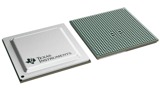
Packaging information
| Package | Pins FCBGA (ALF) | 827 |
| Operating temperature range (°C) -40 to 105 |
| Package qty | Carrier 250 | LARGE T&R |
Features for the TDA4VM
Processor cores:
- C7x floating point, vector DSP, up to 1.0 GHz, 80 GFLOPS, 256 GOPS
- Deep-learning matrix multiply accelerator (MMA), up to 8 TOPS (8b) at 1.0 GHz
- Vision Processing Accelerators (VPAC) with Image Signal Processor (ISP) and multiple vision assist accelerators
- Depth and Motion Processing Accelerators (DMPAC)
- Dual 64-bit Arm
Cortex-A72 microprocessor subsystem at up to 2.0 GHz
- 1MB shared L2 cache per dual-core Cortex-A72 cluster
- 32KB L1 DCache and 48KB L1 ICache per Cortex-A72 core
- Six Arm
Cortex-R5F MCUs at up to 1.0 GHz
- 16K I-Cache, 16K D-Cache, 64K L2 TCM
- Two Arm Cortex-R5F MCUs in isolated MCU subsystem
- Four Arm Cortex-R5F MCUs in general compute partition
- Two C66x floating point DSP, up to 1.35 GHz, 40 GFLOPS, 160 GOPS
- 3D GPU PowerVR Rogue 8XE GE8430, up to 750 MHz, 96 GFLOPS, 6 Gpix/sec
- Custom-designed interconnect
fabric supporting near max processing entitlement
Memory subsystem:
- Up to 8MB of on-chip L3 RAM with
ECC and coherency
- ECC error protection
- Shared coherent cache
- Supports internal DMA engine
- External Memory Interface (EMIF)
module with ECC
- Supports LPDDR4 memory types
- Supports speeds up to 3733 MT/s
- 32-bit data bus with inline ECC up to 14.9GB/s
- General-Purpose Memory Controller (GPMC)
- 512KB on-chip SRAM in MAIN
domain, protected by ECC
Functional Safety:
-
Functional Safety-Compliant targeted (on select part
numbers)
- Developed for functional safety applications
- Documentation available to aid ISO 26262 functional safety system design up to ASIL-D/SIL-3 targeted
- Systematic capability up to ASIL-D/SIL-3 targeted
- Hardware integrity up to ASIL-D/SIL-3 targeted for MCU Domain
- Hardware integrity up to ASIL-B/SIL-2 targeted for Main Domain
- Safety-related
certification
- ISO 26262 planned
- AEC-Q100 qualilfied on part number variants ending in Q1
-
Device security (on select part numbers):
- Secure boot with secure runtime support
- Customer programmable root key, up to RSA-4K or ECC-512
- Embedded hardware security module
- Crypto hardware accelerators –
PKA with ECC, AES, SHA, RNG, DES and 3DES
High speed serial interfaces:
- Integrated ethernet switch
supporting (total of 8 external ports)
- Up to eight 2.5Gb SGMII
- Up to eight RMII (10/100) or RGMII (10/100/1000)
- Up to two QSGMII
- Up to four PCI-Express
(PCIe) Gen3 controllers
- Up to two lanes per controller
- Gen1 (2.5GT/s), Gen2 (5.0GT/s), and Gen3 (8.0GT/s) operation with auto-negotiation
- Two USB 3.0 dual-role device
(DRD) subsystem
- Two enhanced SuperSpeed Gen1 Ports
- Each port supports Type-C switching
- Each port independently configurable as USB host, USB peripheral, or USB DRD
Automotive interfaces:
- Sixteen Modular Controller Area Network (MCAN) modules with full CAN-FD support
- Two CSI2.0 4L RX plus One CSI2.0
4L TX
- 2.5Gbps RX throughput per lane (20Gbps total)
Display subsystem:
- One eDP/DP interface with
Multi-Display Support (MST)
- HDCP1.4/HDCP2.2 high-bandwidth digital content protection
- One DSI TX (up to 2.5K)
- Up to two DPI
Audio interfaces:
- Twelve Multichannel Audio Serial
Port (MCASP) modules
Video acceleration:
- Ultra-HD video, one (3840 × 2160p, 60 fps), or two (3840 × 2160p, 30 fps) H.264/H.265 decode
- Full-HD video, four (1920 × 1080p, 60 fps), or eight (1920 × 1080p, 30 fps) H.264/H.265 decode
- Full-HD video, one (1920 × 1080p,
60 fps), or up to three (1920 × 1080p, 30 fps) H.264 encode
Flash memory interfaces:
- Embedded MultiMediaCard Interface ( eMMC™ 5.1)
- Universal Flash Storage (UFS 2.1) interface with two lanes
- Two Secure Digital 3.0/Secure Digital Input Output 3.0 interfaces (SD3.0/SDIO3.0)
- Two simultaneous flash interfaces
configured as
- One OSPI and one QSPI flash interfaces
- or one HyperBus™ and one QSPI flash interface
System-on-Chip (SoC) architecture:
- 16-nm FinFET technology
- 24 mm × 24 mm, 0.8-mm pitch,
827-pin FCBGA (ALF), enables IPC class 3 PCB routing
TPS6594-Q1 Companion Power Management ICs (PMIC):
- Functional Safety support up to ASIL-D
- Flexible mapping to support different use cases
Description for the TDA4VM
The TDA4VM processor family is based on the evolutionary Jacinto™ 7 architecture, targeted at ADAS and Autonomous Vehicle (AV) applications and built on extensive market knowledge accumulated over a decade of TI’s leadership in the ADAS processor market. The unique combination high-performance compute, deep-learning engine, dedicated accelerators for signal and image processing in an functional safety compliant targeted architecture make the TDA4VM devices a great fit for several industrial applications, such as: Robotics, Machine Vision, Radar, and so on. The TDA4VM provides high performance compute for both traditional and deep learning algorithms at industry leading power/performance ratios with a high level of system integration to enable scalability and lower costs for advanced automotive platforms supporting multiple sensor modalities in centralized ECUs or stand-alone sensors. Key cores include next generation DSP with scalar and vector cores, dedicated deep learning and traditional algorithm accelerators, latest Arm and GPU processors for general compute, an integrated next generation imaging subsystem (ISP), video codec, Ethernet hub and isolated MCU island. All protected by automotive grade safety and security hardware accelerators.
Key Performance Cores Overview
The “C7x” next generation DSP combines TI’s industry leading DSP and EVE cores into a single higher performance core and adds floating point vector calculation capabilities, enabling backward compatibility for legacy code while simplifying software programming. The new “MMA” deep learning accelerator enables performance up to 8 TOPS within the lowest power envelope in the industry when operating at the typical automotive worst case junction temperature of 125°C. The dedicated ADAS/AV hardware accelerators provide vision pre-processing plus distance and motion processing with no impact on system performance.
General Compute Cores and Integration Overview
Separate dual core cluster configuration of Arm Cortex-A72 facilitates multi-OS applications with minimal need for a software hypervisor. Up to six Arm Cortex-R5F subsystems enable low-level, timing critical processing tasks to leave the Arm Cortex-A72’s unencumbered for applications. The integrated “8XE GE8430” GPU offers up to 100 GFLOPS to enable dynamic 3D rendering for enhanced viewing applications. Building on the existing world-class ISP, TI’s 7th generation ISP includes flexibility to process a broader sensor suite, support for higher bit depth, and features targeting analytics applications. Integrated diagnostics and safety features support operations up to ASIL-D/SIL-3 levels while the integrated security features protect data against modern day attacks. To enable systems requiring heavy data bandwidth, a PCIe hub and Gigabit Ethernet switch are included along with CSI-2 ports to support throughput for many sensor inputs. To further the integration, the TDA4VM family also includes an MCU island eliminating the need for an external system microcontroller.