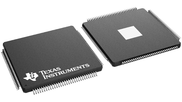
封裝資訊
| 封裝 | 引腳 HLQFP (NNB) | 128 |
| 作業溫度範圍 (°C) -40 to 85 |
| 包裝數量 | 運送包裝 60 | JEDEC TRAY (10+1) |
ADC081500 的特色
- Internal Sample-and-Hold
- Single +1.9V ±0.1V Operation
- Choice of SDR or DDR Output Clocking
- Multiple ADC Synchronization Capability
- Ensured No Missing Codes
- Serial Interface for Extended Control
- Fine Adjustment of Input Full-Scale Range and Offset
- Duty Cycle Corrected Sample Clock
Key Specifications
- Resolution 8 Bits
- Max Conversion Rate 1.5 GSPS (min)
- Bit Error Rate 10-18 (typ)
- ENOB @ 748 MHz Input 7.3 Bits (typ)
- DNL ±0.15 LSB (typ)
- Power Consumption
- Operating 1.2 W (typ)
- Power Down Mode 3.5 mW (typ)
All trademarks are the property of their respective owners.
ADC081500 的說明
The ADC081500 is a low power, high performance CMOS analog-to-digital converter that digitizes signals to 8 bits resolution at sample rates up to 1.7 GSPS. Consuming a typical 1.2 W at 1.5 GSPS from a single 1.9 Volt supply, this device is ensured to have no missing codes over the full operating temperature range. The unique folding and interpolating architecture, the fully differential comparator design, the innovative design of the internal sample-and-hold amplifier and the self-calibration scheme enable a very flat response of all dynamic parameters beyond Nyquist, producing a high 7.3 ENOB with a 748 MHz input signal and a 1.5 GHz sample rate while providing a 10-18 B.E.R. Output formatting is offset binary and the LVDS digital outputs are compatible with IEEE 1596.3-1996, with the exception of an adjustable output offset voltage between 0.8V and 1.2V.
The converter output has a 1:2 demultiplexer that feeds two LVDS buses and reduces the output data rate on each bus to one-half the sample rate.
The converter typically consumes less than 3.5 mW in the Power Down Mode and is available in a 128-lead, thermally enhanced exposed pad HLQFP and operates over the Industrial (-40°C ≤ TA ≤ +85°C) temperature range.
