封裝資訊
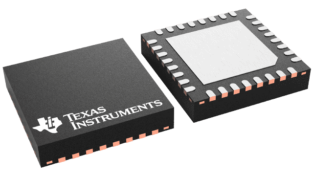
| 封裝 | 引腳 VQFN (RHB) | 32 |
| 作業溫度範圍 (°C) -40 to 85 |
| 包裝數量 | 運送包裝 250 | SMALL T&R |
ADC14X250 的特色
- Resolution: 14-Bit
- Conversion Rate: 250 MSPS
- Performance:
- Input: 240 MHz, –3
dBFS
- SNR: 70.1 dBFS
- Noise Spectral Density: –151.1 dBFS/Hz
- SFDR: 87 dBFS
- Non-HD2 and Non-HD3 SPUR: –92 dBFS
- No Input SNR: 71.1 dBFS
- Input: 240 MHz, –3
dBFS
- Power Dissipation: 584 mW
- Performance Rated up to 105°C (at thermal pad)
- JESD204B Subclass 1 Single Lane Serial Data Interface With Lane Rate Up To 5 Gb/s
- Buffered Analog Inputs
- Differential Input Phase and Amplitude Correction
- Input Sampling Clock Divider (Divide-by-1,2,4,8)
- 4-Wire Serial Peripheral Interface (SPI)
- 32-Pin WQFN Package (5×5 mm, 0.5-mm Pitch)
ADC14X250 的說明
The ADC14X250 device is a monolithic single-channel high performance analog-to-digital converter capable of converting analog input signals into 14-bit digital words with a sampling rate of 250 MSPS. This converter uses a differential pipelined architecture with integrated input buffer to provide excellent dynamic performance and low power consumption across an extended temperature range from –40°C to 105°C as measured at the device’s PCB footprint thermal pad.
The integrated input buffer eliminates charge kickback noise coming from the internal switched capacitor sampling circuits and eases the system-level design of the driving amplifier, anti-aliasing filter, and impedance matching. The buffer can be also be adjusted to correct for phase and amplitude imbalance of the differential input signal path to improve even order harmonic distortion. An input sampling clock divider provides integer divide ratios to simplify system clocking. An integrated low-noise voltage reference eases board level design without requiring external decoupling capacitors. The output digital data is provided through a JESD204B subclass 1 single lane interface from a 32-pin, 5-mm × 5-mm WQFN package. The ADC14X250 operates on 1.2 V, 1.8 V and 3.0 V power supplies. A SPI is available to configure the device that is compatible with 1.2-V to 3-V logic.