封裝資訊
| 封裝 | 引腳 HTQFP (PFP) | 80 |
| 作業溫度範圍 (°C) -40 to 85 |
| 包裝數量 | 運送包裝 96 | JEDEC TRAY (5+1) |
ADS5295 的特色
- Maximum Sample Rate: 100 MSPS
- Designed for Low Power:
- 80 mW per channel at 100 MSPS
- SNR: 70.6 dBFS
- SFDR: 85 dBc at 10 MHz, 100 MSPS
- Serial LVDS ADC Data Outputs:
- One- or Two-Wire Serialized LVDS Outputs per Channel
- One-Wire Interface:
Up to 80 MSPS Sample Rate - Two-Wire Interface:
Up to 100 MSPS Sample Rate
- Digital Processing Block:
- Programmable FIR Decimation Filter and Oversampling to Minimize Harmonic Interference
- Programmable IIR High-Pass Filter to Minimize DC Offset
- Programmable Digital Gain: 0 dB to 12 dB
- Low-Frequency Noise Suppression Mode
- Programmable Mapping Between ADC Input Channels and LVDS Output Pins
- Channel Averaging Mode
- Variety of LVDS Test Patterns to Verify
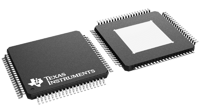
Data Capture by FPGA or Receiver - Package: 12-mm × 12-mm QFP-80
ADS5295 的說明
The ADS5295 is a low-power, 12-bit, 100-MSPS, 8-channel analog-to-digital converter (ADC). Low power consumption and integration of multiple channels in a compact package make the device attractive for very high channel count data acquisition systems.
Serial low-voltage differential signaling (LVDS) outputs reduce the number of interface lines and enable high system integration. The ADC digital data can be output over one or two wires of LVDS pins per channel. At high sample rates, the two-wire interface helps keep the serial data rate low, allowing low-cost field-programmable gate array (FPGA)-based receivers to be used.
The device integrates an internal reference trimmed to accurately match across devices. Best performance is expected to be achieved through the internal reference mode. However, the device can be driven with external references as well.
Several digital functions that are commonly used in systems are included in the device. These functions include a low-frequency suppression mode, digital filtering options, and programmable mapping.
For low input frequency applications, the low-frequency noise suppression mode enables noise suppression at low frequencies and improves signal-to-noise ratio (SNR) in the 1-MHz band near dc by approximately 3 dB. Digital filtering options include low-pass, high-pass, and band-pass digital filters, as well as dc offset removal filters. The device also provides programmable mapping of the LVDS output pins and analog input channels. For applications where the 12-bit ADC SNR is not required, the ADS5295 can be configured as an 8-channel, 10-bit ADC with 10x LVDS serialization to reduce the output data rate.
The device is available in a 12-mm × 12-mm QFP-80 package. The ADS5295 is specified over the –40°C to +85°C operating temperature range.