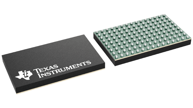
封裝資訊
| 封裝 | 引腳 NFBGA (ZCF) | 135 |
| 作業溫度範圍 (°C) -40 to 85 |
| 包裝數量 | 運送包裝 160 | JEDEC TRAY (5+1) |
AFE5812 的特色
- 8-Channel Complete Analog Front-End
- LNA, VCAT, PGA, LPF, ADC, and CW Mixer
- Programmable Gain Low-Noise Amplifier (LNA)
- 24, 18, 15 dB Gain
- 0.25, 0.5, 0.7 VPP Linear Input Range
- 0.63, 0.7, 0.9 nV/rtHz Input Referred Noise
- Programmable Active Termination
- 40 dB Low Noise Voltage Controlled Attenuator (VCAT)
- 24/30 dB Programmable Gain Amplifier (PGA)
- 3rd Order Linear Phase Low-Pass Filter (LPF)
- 10, 15, 20, 30, 35, 50 MHz
- 14-bit Analog to Digital Converter w/ LVDS output
- 77 dBFS SNR at 65 MSPS
- Noise/Power Optimizations (Without Digital Demodulator)
- 180 mW/CH at 0.75 nV/rtHz, 65 MSPS
- 109 mW/CH at 1.1 nV/rtHz, 40 MSPS
- 107 mW/CH at CW Mode
- Excellent Device-to-Device Gain Matching
- ±0.5 dB(typical) and ±1.1 dB(max)
- Programmable Digital I/Q Demodulator after ADC
- Wide Range Demodulation Frequency
- <1KHz Frequency Resolution
- Decimation Filter Factor M = 1 to 32
- 16xM tap FIR Decimation Filter
- LVDS Rate Reduction after Demodulation
- On-chip RAM with 32 preset Profiles
- Low Harmonic Distortion
- Low Frequency Sonar Signal Processing
- Fast and Consistent Overload Recovery
- Passive Mixer for Continuous Wave Doppler(CWD)
- Low Close-in Phase Noise –156 dBc/Hz at 1 KHz off 2.5 MHz Carrier
- Phase Resolution of 1/16λ
- Support 16X, 8X, 4X and 1X CW Clocks
- 12dB Suppression on 3rd and 5th Harmonics
- Small Package: 15 mm x 9 mm, 135-BGA
- Operation Temperature: -40°C to 85°C
AFE5812 的說明
The AFE5812 is a highly-integrated analog front-end (AFE) solution specifically designed for ultrasound systems in which high performance and small size are required. The AFE5812 integrates a complete time-gain-control (TGC) imaging path and a CWD path. It also enables users to select one of various power/noise combinations to optimize system performance. Therefore, the AFE5812 is a suitable ultrasound AFE solution not only for high-end systems, but also for portable ones.
The AFE5812 contains eight channels of voltage controlled amplifier (VCA), 14-bit and 12-bit ADC, and CW mixer. The VCA includes LNA, VCAT, PGA, and LPF. The LNA gain is programmable to support 250 mVPP to 0.75 VPP input signals. Programmable active termination is also supported by the LNA. The ultra-low noise VCAT provides an attenuation control range of 40 dB and improves overall low-gain SNR, which benefits harmonic imaging and near-field imaging. The PGA provides gain options of 24 and 30 dB. Before the ADC, a LPF can be configured as 10, 15, 20, 30, 35 or 50 MHz to support ultrasound applications with different frequencies. In addition, the signal chain of the AFE5812 can handle signal frequency lower than 100 kHz, which enables the AFE5812 to be used in both sonar and medical applications. The high-performance 14-bit/65-MSPS ADC in the AFE5812 achieves 77 dBFS SNR. It ensures excellent SNR at low chain gain. The ADC’s LVDS outputs enable flexible system integration desired for miniaturized systems.
The AFE5812 integrates a low-power passive mixer and a low-noise summing amplifier to accomplish on-chip CWD beamformer. 16 selectable phase-delays can be applied to each analog input signal. Meanwhile, a unique third- and fifth-order harmonic suppression filter is implemented to enhance CW sensitivity.
The AFE5812 also includes a digital in-phase and quadrature (I/Q) demodulator and a low-pass decimation filter. The main purpose of the demodulation block is to reduce the LVDS data rate and improve overall system power efficiency. The I/Q demodulator can accept ADC output with up to 65 MSPS sampling rate and 14-bit resolution. For example, after digital demodulation and 4× decimation filtering, the data rate for either in-phase or quadrature output is reduced to 16.25 MSPS and the data resolution is improved to 16 bits, consequently. Hence, the overall LVDS trace reduction can be a factor of 2. This demodulator can be bypassed and powered down completely if it is not needed.
The AFE5812 is available in a 15mm × 9mm, 135-pin BGA package, and it is specified for operation from –40°C to 85°C.
