封裝資訊
| 封裝 | 引腳 NFBGA (ZAV) | 289 |
| 作業溫度範圍 (°C) -40 to 85 |
| 包裝數量 | 運送包裝 126 | JEDEC TRAY (5+1) |
AFE58JD16 的特色
- 16-Channel, AFE for Ultrasound Applications:
- Input Attenuator, LNA, LPF, ADC, and
CW Mixer - Digital Time Gain Compensation (DTGC)
- Total Gain Range: 6 dB to 45 dB
- Linear Input Range: 1 VPP
- Input Attenuator, LNA, LPF, ADC, and
- Input Attenuator with DTGC:
- 8-dB to 0-dB Attenuation with 0.125-dB Step
- Supports Matched Impedance for:
- 50-Ω to 800-Ω Source Impedance
- Low-Noise Amplifier (LNA) with DTGC:
- 14-dB to 45-dB Gain with 0.125-dB Step
- Low Input Current Noise: 1.2 pA/√Hz
- 3rd-Order, Linear-Phase, Low-Pass Filter (LPF):
- 10 MHz, 15 MHz, 20 MHz, and 25 MHz
- Analog-to-Digital Converter (ADC):
- 14-Bit ADC: 75-dBFS SNR at 65 MSPS
- 12-Bit ADC: 72-dBFS SNR at 80 MSPS
- LVDS Interface with a Maximum Speed Up to
1 GBPS - Optimized for Noise and Power:
- 90 mW/Ch at 1 nV/√Hz, 65 MSPS
- 55 mW/Ch at 1.45 nV/√Hz, 40 MSPS
- 59 mW/Ch in CW Mode
- Excellent Device-to-Device Gain Matching:
- ±0.5 dB (Typical)
- Low Harmonic Distortion: –60-dBc Level
- Fast and Consistent Overload Recovery
- Continuous Wave (CW) Path with:
- Low Close-In Phase Noise of –148 dBc/Hz
at 1-kHz frequency - Phase Resolution: λ / 16
- Supports 16X, 8X, 4X, and 1X CW Clocks
- Low Close-In Phase Noise of –148 dBc/Hz
- Digital Features:
- Digital I/Q Demodulator after ADC:
- Fractional Decimation Filter M = 1 to 63
with 0.25X Increment Step - Data Throughput Reduction After
Decimation - On-Chip RAM with 32 Preset Profiles
- Fractional Decimation Filter M = 1 to 63
- Digital I/Q Demodulator after ADC:
- 5-Gbps JESD Interface:
- JESD204B Subclass 0, 1, and 2
- 2, 4, or 8 Channels per JESD Lane
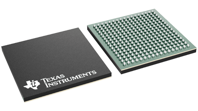
- Small Package: 15-mm × 15-mm NFBGA-289
AFE58JD16 的說明
The AFE58JD16 is a highly-integrated, analog front-end (AFE) solution specifically designed for ultrasound systems where high performance, low power, and small size are required.
To request a full datasheet or other design resources: request AFE58JD16
The AFE58JD16 is an integrated analog front-end (AFE) optimized for medical ultrasound application. The AFE58JD16 is a multichip module (MCM) device with two dies: VCA and ADC_CONV. Each die has total of 16 channels.
Each channel in the VCA die can be configured in two modes: time gain compensation (TGC) mode and continuous wave (CW) mode. In TGC mode, each channel includes an input attenuator (ATTEN), a low-noise amplifier (LNA) with variable-gain, and a third-order, low-pass filter (LPF). The attenuator supports an attenuation range of 8 dB to 0 dB, and the LNA supports gain ranges from 14 dB to 45 dB. The LPF cutoff frequency can be configured at 10 MHz, 15 MHz, 20 MHz, or 25 MHz to support ultrasound applications with different frequencies. In CW mode, each channel includes an LNA with a fixed gain of 18 dB, and a low-power passive mixer with 16 selectable phase delays. Different phase delays can be applied to each analog input signal to perform an on-chip beamforming operation. A harmonic filter in the CW mixer suppresses the third and fifth harmonic to enhance the sensitivity of the CW Doppler measurement. CW mode supports three clock modes: 16X, 8X, and 4X.
Each channel of the ADC_CONV die has a high-performance analog-to-digital converter (ADC) with a programmable resolution of 14 bits or 12 bits. The ADC achieves 75-dBFS signal-to-noise ratio (SNR) in 14-bit mode, and 72-dBFS SNR in 12-bit mode. This ADC provides excellent SNR at low-channel gain. The devices operate at maximum speeds of 65 MSPS and 80 MSPS, providing 14-bit and 12-bit output, respectively. The ADC is designed to scale power with sampling rate. The output interface of the ADC is a low-voltage differential signaling (LVDS) or JESD interface that can easily interface with low-cost field-programmable gate arrays (FPGAs).
The AFE58JD16 includes an optional digital demodulator and JESD204B data packing blocks after the 12- or 14- bit ADC. The digital in-phase and quadrature (I/Q) demodulator with programmable fractional decimation filters accelerates computationally-intensive algorithms at low power. The device also supports an optional JESD204B interface that runs up to 5 Gbps and further reduces the circuit-board routing challenges in high-channel count systems.
The AFE58JD16 also allows various power and noise combinations to be selected for optimizing system performance. Therefore, these devices are suitable ultrasound AFE solutions for systems with strict battery-life requirements. The AFE58JD16 is available in a 15-mm \xD7 15-mm NFBGA-289 package (ZAV package, S-PBGAN289) and is specified for operation from \x9640\xB0C to +85\xB0C. The device pinout is also similar to the AFE5818 family.