封裝資訊
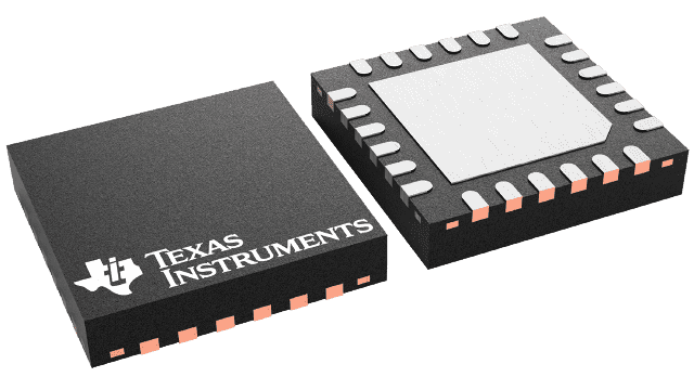
| 封裝 | 引腳 WQFN (RTW) | 24 |
| 作業溫度範圍 (°C) -40 to 85 |
| 包裝數量 | 運送包裝 250 | SMALL T&R |
BQ25896 的特色
- High Efficiency 3-A, 1.5-MHz Switch Mode Buck Charge
- 92.5% Charge Efficiency at 2 A and 90.5% Charge Efficiency at 3 A Charge Current
- Optimize for High Voltage Input (9 V / 12 V)
- Low Power PFM mode for Light Load Operations
- USB On-the-Go (OTG) with Adjustable Output from 4.5 V to 5.5 V
- Selectable 500-KHz / 1.5-MHz Boost Converter with up-to 2 A Output
- 93% Boost Efficiency at 5 V at 1 A Output
- Accurate Hiccup Mode Overcurent Protection
- Support down-to 2.5V Battery
- Support PWM only or PFM/PWM control for Light Load Efficiency
- Single Input to Support USB
Input and Adjustable High Voltage Adapters
- Support 3.9-V to 14-V Input Voltage Range
- Input Current Limit (100 mA to 3.25 A with 50-mA resolution) to Support USB2.0, USB3.0 standard and High Voltage Adapters
- Maximum Power Tracking by Input Voltage Limit up-to 14V for Wide Range of Adapters
- Input Current Optimizer (ICO) to Maximize Input Power without Overloading Adapters
- Resistance Compensation (IRCOMP) from Charger Output to Cell Terminal
- Highest Battery Discharge Efficiency with 11-mΩ Battery Discharge MOSFET up to 9 A
- Integrated ADC for
System Monitor
(Voltage, Temperature, Charge Current) - Narrow VDC (NVDC) Power Path
Management
- Instant-on Works with No Battery or Deeply Discharged Battery
- Ideal Diode Operation in Battery Supplement Mode
- BATFET Control to Support Ship Mode, Wake Up, and Full System Reset
- Flexible Autonomous and I2C Mode for Optimal System Performance
- High Integration includes all MOSFETs, Current Sensing and Loop Compensation
- 12-µA Low Battery Leakage Current to Support Ship Mode
- High Accuracy
- ±0.5% Charge Voltage Regulation
- ±5% Charge Current Regulation
- ±7.5% Input Current Regulation
- Safety
- Battery Temperature Sensing for Charge and Boost Mode
- Thermal Regulation and Thermal Shutdown
BQ25896 的說明
The bq25896 is a highly-integrated 3-A switch-mode battery charge management and system power path management device for single cell Li-Ion and Li-polymer battery. The devices support high input voltage fast charging. The low impedance power path optimizes switch-mode operation efficiency, reduces battery charging time and extends battery life during discharging phase. The I2C Serial interface with charging and system settings makes the device a truly flexible solution.
The bq25896 is a highly-integrated 3-A switch-mode battery charge management and system power path management device for single cell Li-Ion and Li-polymer battery. It features fast charging with high input voltage support for a wide range of smartphone, tablet and portable devices. Its low impedance power path optimizes switch-mode operation efficiency, reduces battery charging time and extends battery life during discharging phase. It also integrates Input Current Optimizer (ICO) and Resistance Compensation (IRCOMP) to deliver maximum charging power to battery. The solution is highly integrated with input reverse-blocking FET (RBFET, Q1), high-side switching FET (HSFET, Q2), low-side switching FET (LSFET, Q3), and battery FET (BATFET, Q4) between system and battery. It also integrates the bootstrap diode for the high-side gate drive and battery monitor for simplified system design. The I2C serial interface with charging and system settings makes the device a truly flexible solution.
The device supports a wide range of input sources and takes the result from detection circuit in the system, such as USB PHY device. The input current and voltage regulation selection is compactible with USB 2.0 and USB 3.0 power spec. In addition, the Input Current Optimizer (ICO) supports the detection of maximum power point detection of the input source without overload. The device also meets USB On-the-Go (OTG) operation power rating specification by supplying 5 V (Adjustable 4.5V-5.5V) on VBUS with current limit up to 2 A.
The power path management regulates the system slightly above battery voltage but does not drop below 3.5V minimum system voltage (programmable). With this feature, the system maintains operation even when the battery is completely depleted or removed. When the input current limit or voltage limit is reached, the power path management automatically reduces the charge current to zero. As the system load continues to increase, the power path discharges the battery until the system power requirement is met. This Supplemental Mode operation prevents overloading the input source.
The device initiates and completes a charging cycle without software control. It automatically detects the battery voltage and charges the battery in three phases: pre-conditioning, constant current and constant voltage. At the end of the charging cycle, the charger automatically terminates when the charge current is below a preset limit in the constant voltage phase. When the full battery falls below the recharge threshold, the charger will automatically start another charging cycle.
The charger provides various safety features for battery charging and system operations, including battery temperature negative thermistor monitoring, charging safety timer and overvoltage/overcurrent protections. The thermal regulation reduces charge current when the junction temperature exceeds 120°C (programmable). The STAT output reports the charging status and any fault conditions. The PG output indicates if a good power source is present. The INT immediately notifies host when fault occurs.
The device also provides a 7-bit analog-to-digital converter (ADC) for monitoring charge current and input/battery/system (VBUS, BAT, SYS, TS) voltages. The QON pin provides BATFET enable/reset control to exit low power ship mode or full system reset function.
The device family is available in 24-pin, 4 x 4 mm2 x 0.75 mm thin WQFN package.