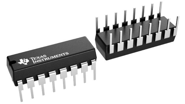
封裝資訊
| 封裝 | 引腳 PDIP (N) | 16 |
| 作業溫度範圍 (°C) -55 to 125 |
| 包裝數量 | 運送包裝 25 | TUBE |
CD74HCT40105 的特色
- Independent Asynchronous Inputs and Outputs
- Expandable in Either Direction
- Reset Capability
- Status Indicators on Inputs and Outputs
- Three-State Outputs
- Shift-Out Independent of Three-State Control
- Fanout (Over Temperature Range)
- Standard Outputs . . . . . . . . . . . . . . . 10 LSTTL Loads
- Bus Driver Outputs . . . . . . . . . . . . . 15 LSTTL Loads
- Wide Operating Temperature Range . . . -55°C to 125°C
- Balanced Propagation Delay and Transition Times
- Significant Power Reduction Compared to LSTTL Logic ICs
- HC Types
- 2V to 6V Operation
- High Noise Immunity: NIL = 30%, NIH = 30% of VCC at VCC = 5V
- HCT Types
- 4.5V to 5.5V Operation
- Direct LSTTL Input Logic Compatibility, VIL = 0.8V (Max), VIH = 2V (Min)
- CMOS Input Compatibility, Il ≤ 1µA at VOL, VOH
- Applications
- Bit-Rate Smoothing
- CPU/Terminal Buffering
- Data Communications
- Peripheral Buffering
- Line Printer Input Buffers
- Auto-Dialers
- CRT Buffer Memories
- Radar Data Acquisition
CD74HCT40105 的說明
The ’HC40105 and ’HCT40105 are high-speed silicon-gate CMOS devices that are compatible, except for "shift-out" circuitry, with the CD40105B. They are low-power first-in-out (FIFO) "elastic" storage registers that can store 16 four-bit words. The 40105 is capable of handling input and output data at different shifting rates. This feature makes particularly useful as a buffer between asynchronous systems.
Each work position in the register is clocked by a control flip-flop, which stores a marker bit. A "1" signifies that the position’s data is filled and a "0" denotes a vacancy in that position. The control flip-flop detects the state of the preceding flip-flop and communicates its own status to the succeeding flip-flop. When a control flip-flop is in the "0" state and sees a "1" in the preceeding flip-flop, it generates a clock pulse that transfers data from the preceding four data latches into its own four data latches and resets the preceding flip-flop to "0". The first and last control flip-flops have buffered outputs. Since all empty locations "bubble" automatically to the input end, and all valid data ripple through to the output end, the status of the first control flip-flop (DATA-IN READY) indicates if the FIFO is full, and the status of the last flip-flop (DATA-OUT READY) indicates if the FIFO contains data. As the earliest data are removed from the bottom of the data stack (the output end), all data entered later will automatically propagate (ripple) toward the output.
