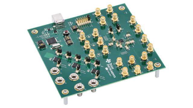
CDCUN1208LPEVM 的特色
- Easy-to-use evaluation module to buffer low phase noise clocks up to 400 MHz
- Easy device programming via host-powered USB port
- Easy device programming via control pins
- Rapid configuration through provided EVM Control Software
- Can be powered from the USB port, or by an external 3.3V/2.5V/1.8V power supply
- Single-ended or differential input
CDCUN1208LPEVM 的說明
The CDCUN1208LP is a 2:8 fan-out buffer featuring a wide operating supply range, two universal differential/ single ended inputs, and universal outputs (HCSL, LVDS, or LVCMOS) with clock edge rate control. One of the device inputs includes a divider that provides divide values of /1, /2, /4, and /8.
The device is offered in a 32 pin QFN package. The CDCUN1208LP is flexible and easy to use. The application configures the device by setting the state of certain pins at device power-up. Alternately, the application can configure the device via SPI/I2C. The CDCUN1208LP delivers excellent additive jitter performance, and low power consumption. The output section includes four dedicated output supply pins enabling the operation of output ports from different power supply domains. This provides the ability to clock devices switching at different LVCMOS levels without the need for external logic level translation circuitry.