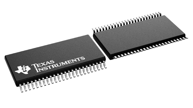
封裝資訊
| 封裝 | 引腳 TSSOP (DGG) | 48 |
| 作業溫度範圍 (°C) -40 to 85 |
| 包裝數量 | 運送包裝 40 | TUBE |
CDCVF857 的特色
- Spread-Spectrum Clock Compatible
- Operating Frequency: 60 MHz to 220 MHz
- Low Jitter (Cycle-Cycle): ±35 ps
- Low Static Phase Offset: ±50 ps
- Low Jitter (Period): ±30 ps
- 1-to-10 Differential Clock Distribution (SSTL2)
- Best in Class for VOX = VDD/2 ±0.1 V
- Operates From Dual 2.6-V or 2.5-V Supplies
- Available in a 40-Pin MLF Package, 48-Pin TSSOP Package, 56-Ball MicroStar Junior™ BGA Package
- Consumes < 100-µA Quiescent Current
- External Feedback Pins (FBIN, FBIN) Are Used to Synchronize the Outputs to the Input Clocks
- Meets/Exceeds JEDEC Standard (JESD82-1) For DDRI-200/266/333 Specification
- Meets/Exceeds Proposed DDRI-400 Specification (JESD82-1A)
- Enters Low-Power Mode When No CLK Input Signal Is Applied or PWRDWN Is Low
- APPLICATIONS
- DDR Memory Modules (DDR400/333/266/200)
- Zero-Delay Fan-Out Buffer
MicroStar Junior is a trademark of Texas Instruments.
CDCVF857 的說明
The CDCVF857 is a high-performance, low-skew, low-jitter, zero-delay buffer that distributes a differential clock input pair (CLK, CLK) to 10 differential pairs of clock outputs (Y[0:9], Y[0:9]) and one differential pair of feedback clock outputs (FBOUT, FBOUT). The clock outputs are controlled by the clock inputs (CLK, CLK), the feedback clocks (FBIN, FBIN), and the analog power input (AVDD). When PWRDWN is high, the outputs switch in phase and frequency with CLK. When PWRDWN is low, all outputs are disabled to a high-impedance state (3-state) and the PLL is shut down (low-power mode). The device also enters this low-power mode when the input frequency falls below a suggested detection frequency that is below 20 MHz (typical 10 MHz). An input frequency detection circuit detects the low frequency condition and, after applying a >20-MHz input signal, this detection circuit turns the PLL on and enables the outputs.
When AVDD is strapped low, the PLL is turned off and bypassed for test purposes. The CDCVF857 is also able to track spread spectrum clocking for reduced EMI.
Because the CDCVF857 is based on PLL circuitry, it requires a stabilization time to achieve phase-lock of the PLL. This stabilization time is required following power up. The CDCVF857 is characterized for both commercial and industrial temperature ranges.
