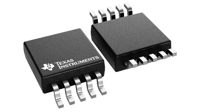
封裝資訊
| 封裝 | 引腳 VSSOP (DGS) | 10 |
| 作業溫度範圍 (°C) -40 to 125 |
| 包裝數量 | 運送包裝 2,500 | LARGE T&R |
DAC8563T 的特色
- Relative Accuracy: 4 LSB INL at 16 Bits
- Low Glitch Impulse: 0.1 nV-s
- Bidirectional Reference Pin: Input or 2.5-V Output
- 4-ppm/°C Temperature Drift (Typ)
- Power-On Reset to Zero Scale or Mid-Scale
- Low-Power: 4 mW at 5-V AVDD
- Wide Power-Supply Range: 2.7 V to 5.5 V
- 50-MHz SPI With Schmitt-Triggered Inputs
- LDAC and CLR Functions
- Output Buffer With Rail-to-Rail Operation
- Pin-to-Pin Compatible With DAC8562 Family
- 5-V TTL I/O Enabled
- Packages: WSON-10 (3 mm × 3 mm), VSSOP-10
- Temperature Range: –40°C to 125°C
DAC8563T 的說明
The DAC856xT, DAC816xT, and DAC756xT devices are low-power, voltage-output, dual-channel, 16-, 14-, and 12-bit digital-to-analog converters (DACs), respectively. These devices include a 2.5-V, 4-ppm/°C internal reference, giving a full-scale output voltage range of 2.5 V or 5 V. The internal reference has an initial accuracy of ±5 mV and can source or sink up to 20 mA at the VREFIN/VREFOUT pin.
These devices are monotonic, providing excellent linearity and minimizing undesired code-to-code transient voltages (glitch). They use a versatile three-wire serial interface that operates at clock rates up to 50 MHz. The interface is compatible with standard SPI™, QSPI™, Microwire, and digital signal processor (DSP) interfaces. The DACxx62T devices incorporate a power-on-reset circuit that ensures the DAC output powers up and remains at zero scale until a valid code is written to the device, whereas the DACxx63T devices similarly power up at mid-scale. These devices contain a power-down feature that reduces current consumption to typically 550 nA at 5 V. The low power consumption, internal reference, and small footprint make these devices ideal for portable, battery-operated equipment.
The DACxx62T devices are drop-in and function-compatible with each other, as are the DACxx63T devices. The entire family is available in VSSOP-10 and WSON-10 packages.
