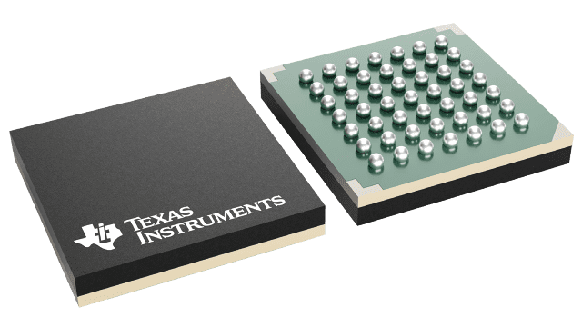
封裝資訊
| 封裝 | 引腳 NFBGA (NZA) | 49 |
| 作業溫度範圍 (°C) -40 to 85 |
| 包裝數量 | 運送包裝 416 | EIAJ TRAY (10+1) |
SCAN921224 的特色
- IEEE 1149.1 (JTAG) Compliant and At-Speed BIST Test Mode
- Clock Recovery From PLL Lock to Random Data Patterns
- Ensured Transition Every Data Transfer Cycle
- Chipset (Tx + Rx) Power Consumption < 500 mW (typ) @ 66 MHz
- Single Differential Pair Eliminates Multi-Channel Skew
- Flow-Through Pinout for Easy PCB Layout
- 660 Mbps Serial Bus LVDS Data Rate (at 66 MHz Clock)
- 10-bit Parallel Interface for 1 Byte Data Plus 2 Control Bits
- Synchronization Mode and LOCK Indicator
- Programmable Edge Trigger on Clock
- High Impedance on Receiver Inputs when Power is Off
- Bus LVDS Serial Output Rated for 27Ω Load
- Small 49-Lead NFBGA Package
All trademarks are the property of their respective owners.
SCAN921224 的說明
The SCAN921023 transforms a 10-bit wide parallel LVCMOS/LVTTL data bus into a single high speed Bus LVDS serial data stream with embedded clock. The SCAN921224 receives the Bus LVDS serial data stream and transforms it back into a 10-bit wide parallel data bus and recovers parallel clock. Both devices are compliant with IEEE 1149.1 Standard Test Access Port and Boundary Scan Architecture with the incorporation of the defined boundary-scan test logic and test access port consisting of Test Data Input (TDI), Test Data Out (TDO), Test Mode Select (TMS), Test Clock (TCK), and the optional Test Reset (TRST). IEEE 1149.1 features provide the designer or test engineer access to the backplane or cable interconnects and the ability to verify differential signal integrity to enhance their system test strategy. The pair of devices also features an at-speed BIST mode which allows the interconnects between the Serializer and Deserializer to be verified at-speed.
The SCAN921023 transmits data over backplanes or cable. The single differential pair data path makes PCB design easier. In addition, the reduced cable, PCB trace count, and connector size tremendously reduce cost. Since one output transmits clock and data bits serially, it eliminates clock-to-data and data-to-data skew. The powerdown pin saves power by reducing supply current when not using either device. Upon power up of the Serializer, you can choose to activate synchronization mode or allow the Deserializer to use the synchronization-to-random-data feature. By using the synchronization mode, the Deserializer will establish lock to a signal within specified lock times. In addition, the embedded clock ensures a transition on the bus every 12-bit cycle. This eliminates transmission errors due to charged cable conditions. Furthermore, you may put the SCAN921023 output pins into TRI-STATE to achieve a high impedance state. The PLL can lock to frequencies between 20 MHz and 66 MHz.
