封裝資訊
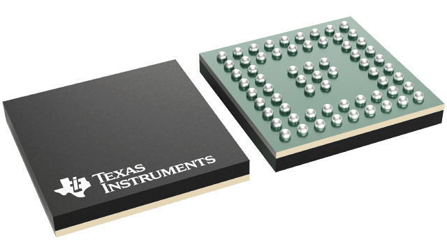
| 封裝 | 引腳 NFBGA (ZXH) | 64 |
| 作業溫度範圍 (°C) -40 to 85 |
| 包裝數量 | 運送包裝 2,500 | LARGE T&R |
SN65DSI85 的特色
- Implements MIPI D-PHY version 1.00.00 physical layer front-end and display serial interface (DSI) version 1.02.00
- Dual-channel DSI receiver configurable for one, two, three, or four D-PHY data lanes per channel operating up to 1 Gbps per lane
- Supports 18-bpp and 24-bpp DSI video packets with RGB666 and RGB888 formats
- Suitable for 60 fps WQXGA 2560 × 1600 resolution at 18-bpp and 24-bpp color, and WUXGA 1920 × 1200 resolution with 3D graphics at 60 fps (120 fps equivalent)
- MIPI® front-end configurable for single-channel or dual-channel DSI configurations
- FlatLink™ output configurable for single-link or dual-link LVDS
- Supports dual-channel DSI ODD or EVEN and LEFT or RIGHT operating modes
- Supports two single-channel DSI to two single-link LVDS operating mode
- LVDS output clock range of 25 MHz to 154 MHz in dual-link or single-link mode
- LVDS pixel clock may be sourced from free-running continuous D-PHY clock or external reference clock (REFCLK)
- 1.8-V main VCC power supply
- Low-power features include shutdown mode, reduced LVDS output voltage swing, common mode, and MIPI® ultra-low power state (ULPS) support
- LVDS channel swap, LVDS pin order reverse feature for ease of PCB routing
- ESD rating ±2 kV (HBM)
- Packaged in 64-pin 5 mm x 5 mm nFBGA (ZXH)
- Temperature range: –40°C to 85°C
SN65DSI85 的說明
The SN65DSI85 DSI to FlatLink bridge features a dual-channel MIPI D-PHY receiver front-end configuration with 4 lanes per channel operating at 1 Gbps per lane; a maximum input bandwidth of 8 Gbps. The bridge decodes MIPI DSI 18-bpp RGB666 and 24-bpp RGB888 packets and converts the formatted video data stream to a FlatLink compatible LVDS output operating at pixel clocks operating from 25 MHz to 154 MHz, offering a Dual-Link LVDS, Single-Link LVDS, or two Single-Link LVDS interface(s) with four data lanes per link.
The SN65DSI85 is well suited for WQXGA (2560 × 1600) at 60 frames per second, as well as 3D Graphics at WUXGA and True HD (1920 × 1080) resolutions at an equivalent 120 fps with up to 24 bits-per-pixel. Partial line buffering is implemented to accommodate the data stream mismatch between the DSI and LVDS interfaces.
Designed with industry-compliant interface technology, the SN65DSI85 is compatible with a wide range of micro-processors, and is designed with a range of power management features including low-swing LVDS outputs, and the MIPI® defined ultra-low power state (ULPS) support.
The SN65DSI85 is implemented in a small outline 5-mm × 5-mm nFBGA at 0.5-mm pitch package, and operates across a temperature range from –40°C to 85°C.
