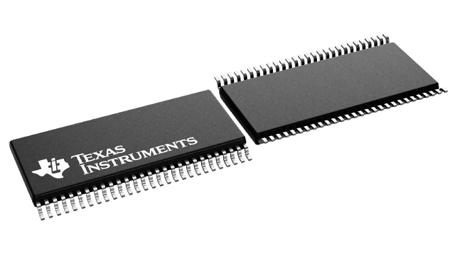
封裝資訊
| 封裝 | 引腳 TSSOP (DGG) | 56 |
| 作業溫度範圍 (°C) -40 to 85 |
| 包裝數量 | 運送包裝 2,000 | LARGE T&R |
SN74ALVCH162268 的特色
- Member of the Texas Instruments Widebus™ Family
- Operates From 1.65 V to 3.6 V VCC
- Max tpd of 4.8 ns at 3.3 V VCC
- ±24 mA Output Drive at 3.3 V VCC
- B-Port Outputs Have Equivalent 26-
 Series Resistors, So No External Resistors Are Required
 - Bus Hold on Data Inputs Eliminates the Need for External Pullup/Pulldown Resistors
- Latch-Up Performance Exceeds 250 mA Per JESD 17
- ESD Protection Exceeds JESD 22
- 2000-V Human-Body Model (A114-A)
- 200-V Machine Model (A115-A)
Widebus is a trademark of Texas Instruments.
SN74ALVCH162268 的說明
This 12-bit to 24-bit registered bus exchanger is designed for 1.65-V to 3.6-V VCC operation.
The SN74ALVCH162268 is used for applications in which data must be transferred from a narrow high-speed bus to a wide, lower-frequency bus.
The device provides synchronous data exchange between the two ports. Data is stored in the internal registers on the low-to-high transition of the clock (CLK) input when the appropriate clock-enable (CLKEN)\ inputs are low. The select (SEL)\ line is synchronous with CLK and selects 1B or 2B input data for the A outputs.
For data transfer in the A-to-B direction, a two-stage pipeline is provided in the A-to-1B path, with a single storage register in the A-to-2B path. Proper control of these inputs allows two sequential 12-bit words to be presented synchronously as a 24-bit word on the B port. Data flow is controlled by the active-low output enables (OEA\, OEB\). These control terminals are registered, so bus direction changes are synchronous with CLK.
The B outputs, which are designed to sink up to 12 mA, include equivalent 26- resistors to reduce overshoot and undershoot.
To ensure the high-impedance state during power up or power down, a clock pulse should be applied as soon as possible and OE\ should be tied to VCC through a pullup resistor; the minimum value of the resistor is determined by the current-sinking capability of the driver. Due to OE\ being routed through a register, the active state of the outputs cannot be determined prior to the arrival of the first clock pulse.
Active bus-hold circuitry holds unused or undriven inputs at a valid logic state. Use of pullup or pulldown resistors with the bus-hold circuitry is not recommended.
