封裝資訊
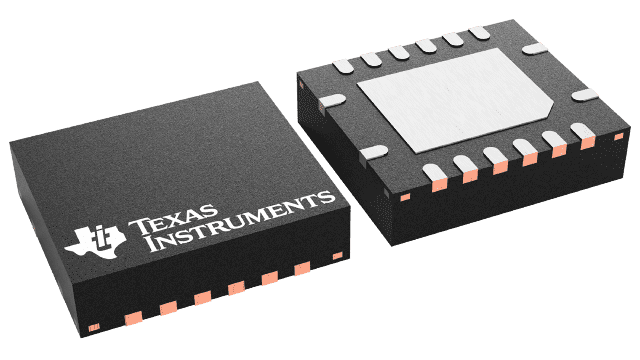
| 封裝 | 引腳 VQFN (RGY) | 16 |
| 作業溫度範圍 (°C) -40 to 85 |
| 包裝數量 | 運送包裝 3,000 | LARGE T&R |
SN74CBT3257C 的特色
- Undershoot Protection for Off-Isolation on A and B Ports Up To .2 V
- Bidirectional Data Flow, With Near-Zero Propagation Delay
- Low ON-State Resistance (ron) Characteristics (ron = 3
 Typical)
 - Low Input/Output Capacitance Minimizes Loading and Signal Distortion (Cio(OFF) = 5.5 pF Typical)
- Data and Control Inputs Provide Undershoot Clamp Diodes
- Low Power Consumption (ICC = 3 µA Max)
- VCC Operating Range From 4 V to 5.5 V
- Data I/Os Support 0 to 5-V Signaling Levels (0.8-V, 1.2-V, 1.5-V, 1.8-V, 2.5-V, 3.3-V, 5-V)
- Control Inputs Can be Driven by TTL or 5-V/3.3-V CMOS Outputs
- Ioff Supports Partial-Power-Down Mode Operation
- Latch-Up Performance Exceeds 100 mA Per JESD 78, Class II
- ESD Performance Tested Per JESD 22
- 2000-V Human-Body Model (A114-B, Class II)
- 1000-V Charged-Device Model (C101)
- Supports I2C Bus Expansion
- Supports Both Digital and Analog Applications: USB Interface, Bus Isolation, Low-Distortion Signal Gating
SN74CBT3257C 的說明
The SN74CBT3257C is a high-speed TTL-compatible FET multiplexer/demultiplexer with low ON-state resistance (ron), allowing for minimal propagation delay. Active Undershoot-Protection Circuitry on the A and B ports of the SN74CBT3257C provides protection for undershoot up to –2 V by sensing an undershoot event and ensuring that the switch remains in the proper OFF state.
The SN74CBT3257C is a 4-bit 1-of-2 multiplexer/demultiplexer with a single output-enable (OE\) input. The select (S) input controls the data path of the multiplexer/demultiplexer. When OE\ is low, the multiplexer/demultiplexer is enabled and the A port is connected to the B port, allowing bidirectional data flow between ports. When OE\ is high, the multiplexer/demultiplexer is disabled and a high-impedance state exists between the A and B ports.
This device is fully specified for partial-power-down applications using Ioff. The Ioff feature ensures that damaging current will not backflow through the device when it is powered down. The device has isolation during power off.
To ensure the high-impedance state during power up or power down, OE\ should be tied to VCC through a pullup resistor; the minimum value of the resistor is determined by the current-sinking capability of the driver.