封裝資訊
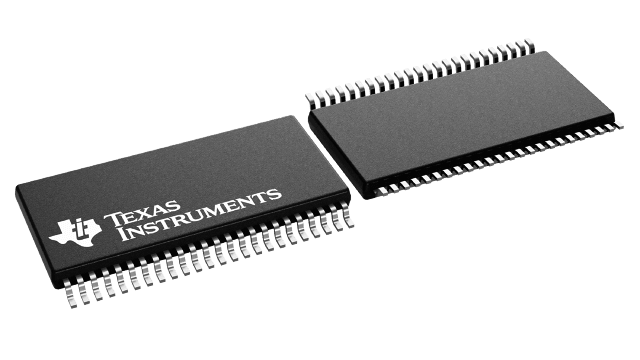
| 封裝 | 引腳 TSSOP (DGG) | 48 |
| 作業溫度範圍 (°C) -40 to 85 |
| 包裝數量 | 運送包裝 2,000 | LARGE T&R |
SN74LVTH16373 的特色
- Members of the Texas Instruments Widebus™ Family
- State-of-the-Art Advanced BiCMOS Technology (ABT) Design for 3.3-V Operation and Low Static-Power Dissipation
- Support Mixed-Mode Signal Operation (5-V Input and Output Voltages With 3.3-V VCC)
- Support Unregulated Battery Operation Down to 2.7 V
- Typical VOLP (Output Ground Bounce) <0.8 V at VCC = 3.3 V, TA = 25°C
- Ioff and Power-Up 3-State Support Hot Insertion
- Bus Hold on Data Inputs Eliminates the Need for External Pullup/Pulldown Resistors
- Distributed VCC and GND Pins Minimize High-Speed Switching Noise
- Flow-Through Architecture Optimizes PCB Layout
- Latch-Up Performance Exceeds 500 mA Per JESD 17
- ESD Protection Exceeds JESD 22
- 2000-V Human-Body Model (A114-A)
- 200-V Machine Model (A115-A)
Widebus is a trademark of Texas Instruments.
SN74LVTH16373 的說明
The 'LVTH16373 devices are 16-bit transparent D-type latches with 3-state outputs designed for low-voltage (3.3-V) VCC operation, but with the capability to provide a TTL interface to a 5-V system environment. These devices are particularly suitable for implementing buffer registers, I/O ports, bidirectional bus drivers, and working registers.
These devices can be used as two 8-bit latches or one 16-bit latch. When the latch-enable (LE) input is high, the Q outputs follow the data (D) inputs. When LE is taken low, the Q outputs are latched at the levels set up at the D inputs.
A buffered output-enable (OE) input can be used to place the eight outputs in either a normal logic state (high or low logic levels) or a high-impedance state. In the high-impedance state, the outputs neither load nor drive the bus lines significantly. The high-impedance state and the increased drive provide the capability to drive bus lines without interface or pullup components.
OE does not affect internal operations of the latch. Old data can be retained or new data can be entered while the outputs are in the high-impedance state.
Active bus-hold circuitry holds unused or undriven inputs at a valid logic state. Use of pullup or pulldown resistors with the bus-hold circuitry is not recommended.
When VCC is between 0 and 1.5 V, the devices are in the high-impedance state during power up or power down. However, to ensure the high-impedance state above 1.5 V, OE should be tied to VCC through a pullup resistor; the minimum value of the resistor is determined by the current-sinking capability of the driver.
These devices are fully specified for hot-insertion applications using Ioff and power-up 3-state. The Ioff circuitry disables the outputs, preventing damaging current backflow through the devices when they are powered down. The power-up 3-state circuitry places the outputs in the high-impedance state during power up and power down, which prevents driver conflict.