封裝資訊
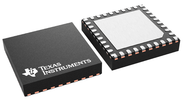
| 封裝 | 引腳 VQFN (RHB) | 32 |
| 作業溫度範圍 (°C) -40 to 125 |
| 包裝數量 | 運送包裝 3,000 | LARGE T&R |
TPS25833-Q1 的特色
- AEC-Q100 qualified for automotive applications:
- Temperature grade 1: –40°C to +125°C, TA
- HBM ESD classification level H2
- CDM ESD classification level C5
-
Functional Safety-Capable
- Documentation available to aid functional safety system design
- Synchronous buck DC/DC regulator
- Input voltage range: 4.5 V to 36 V
- Output current: 3.5 A
- 5.1-V output voltage with ±1% accuracy
- Current mode control
- Adjustable frequency: 300 kHz to 2.2 MHz
- Frequency synchronization to external clock
- FPWM with spread-spectrum dithering
- Internal compensation for ease of use
- Compliant to USB-IF standards
-
USB Type-C Rev 1.3
- CC logic, VCONN source and discharge
- USB cable polarity detection (POL)
- CDP/SDP Mode per USB BC1.2
- Automatic DCP modes (TPS25833-Q1 only)
- DCP shorted mode and YD/T 1591-2009
- 2.7-V divider 3 mode
- 1.2-V mode
-
USB Type-C Rev 1.3
- Optimized for USB power and communication
- User-programmable USB current limit
- Cable droop compensation up to 1.5 V
- High bandwidth data switches on DP and DM (TPS25832-Q1 only)
- NTC input for intelligent thermal management (TPS25833-Q1 only)
- Integrated protection
- DP_IN and DM_IN Short-to-VBUS protection
- DP_IN, DM_IN, CCx IEC 61000-4-2 rated
- ±8-kV contact and ±15-kV air discharge
- Fault flag reports
- 32-pin QFN package with wettable flank
TPS25833-Q1 的說明
The TPS2583x-Q1 is a USB Type-C and BC1.2 charging port controller that includes a synchronous DC/DC converter. With cable droop compensation, the VBUS voltage remains constant regardless of load current, ensuring connected portable devices charge at optimal current and voltage.
The TPS25832-Q1 includes high bandwidth analog switches for DP and DM pass-through, while the TPS25833-Q1 includes a thermistor input pin and thermal warning flag for user programmable thermal overload protection.
The synchronous buck regulator operates with current mode control and is internally compensated to simplify the design. A resistor on the RT pin sets the switching frequency between 300 kHz and 2.2 MHz. Operating below 400 kHz results in better system efficiency. Operation above 2.1 MHz avoids the AM radio bands and allows for use of a smaller inductor.
The TPS2583x-Q1 integrates standard USB Type-C port controller functionality including Configuration Channel (CC) logic for 3-A and 1.5-A current advertisement. Battery Charging (Rev. 1.2) integration provides the required electrical signatures necessary for non-Type-C, legacy USB devices that use USB data line signaling to determine USB port current sourcing capabilities.
A precision current sense amplifier is included for user programmable cable droop compensation and current limit tuning. Cable compensation aids portable devices in charging at optimum current and voltage under heavy loads by changing the buck regulator output voltage linearly with load current to counteract the voltage drop due to wire resistance in automotive cabling. The VBUS voltage measured at a connected portable device remains approximately constant, regardless of load current, allowing the portable device’s battery charger to work optimally.
The USB specifications require current limiting of USB charging ports, but give system designers reasonable flexibility to choose overcurrent protection levels based on system requirements. The TPS2583x-Q1 uses a novel two-threshold current limit circuit allowing system designers to either program average current limit protection of the buck regulator, or optionally, current limit using an external NMOS between the CSN/OUT and BUS pins. The NFET implementation enables the TPS2583x-Q1 buck regulator to supply a 5-V output for other loads during an overcurrent fault condition on the USB port.
The TPS25832-Q1 includes high bandwidth analog switches for DP and DM pass-through. The TPS25833-Q1 includes a thermistor input pin and thermal warning flag for user programmable thermal overload protection.
Integrated protection features include cycle-by-cycle current limit, hiccup short-circuit protection, undervoltage lockout, VBUS overvoltage and overcurrent, CC overvoltage and overcurrent, data line (Dx) short-to-VBUS and die overtemperature protection.