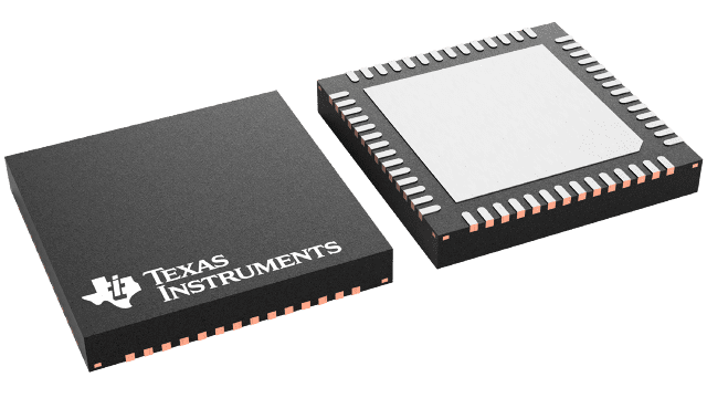
封裝資訊
| 封裝 | 引腳 VQFN (RSH) | 56 |
| 作業溫度範圍 (°C) 0 to 85 |
| 包裝數量 | 運送包裝 2,500 | LARGE T&R |
VSP5611 的特色
- Four-Channel CCD/CMOS Signal: 2-Channel, 3-Channel, and 4-Channel Selectable
- Power Supply: 3.3 V Only, Typ
(Built-in LDO, 3.3 V to 1.8 V) - Maximum Conversion Rate:
- VSP5610: 35 MSPS
- VSP5611: 50 MSPS
- VSP5612: 70 MSPS
- 16-Bit Resolution
- CDS/SH Selectable
- Maximum Input Signal Range: 2.0 V
- Analog and Digital Hybrid Gain:
- Analog Gain: 0.5 V/V to 3.5 V/V in
3/64-V/V Steps - Digital Gain: 1 V/V to 2 V/V in
1/256-V/V Steps
- Analog Gain: 0.5 V/V to 3.5 V/V in
- Offset Correction DAC: ±250 mV, 8-Bit
- Standard LVDS/CMOS Selectable Output:
- LVDS:Data Channel: 2-Channel, 3-ChannelClock Channel: 1-Channel8-Bit/7-Bit Serializer Selectable
- CMOS: 4 Bits × 4, 8 Bits × 2
- Timing Generator:
- Fast Transfer Clock: Eight Signals
- Slow Transfer Clock: Six Signals
- Timing Adjustment Resolution: tMCLK/48
- Input Clamp/Input Reference Level Internal/External Selectable
- Reference DAC: 0.5 V, 1.1 V, 1.5 V, 2 V
- SPI™: Three-Wire Serial
- GPIO: Four-Port
- Copiers
- Facsimile Machines
- Scanners
SPI is a trademark of Motorola.
All other trademarks are the property of their respective owners.
VSP5611 的說明
The VSP5610/11/12 are high-speed, high-performance, 16-bit analog-to-digital-converters (ADCs) that have four independent sampling circuit channels for multi-output charge-coupled device (CCD) and complementary metal oxide semiconductor (CMOS) line sensors. Pixel data from the sensor are sampled by the sample/hold (SH) or correlated double sampler (CDS) circuit, and are then converted to digital data by an ADC. Data output is selectable in low-voltage differential signaling (LVDS) or CMOS modes.
The VSP5610/11/12 include a programmable gain to support the pixel level inflection caused by luminance. The integrated digital-to-analog-converter (DAC) can be used to adjust the offset level for the analog input signal. Furthermore, the timing generator (TG) is integrated in these devices for the control of sensor operation.
The VSP5610/11/12 use 1.65 V to 1.95 V for the core voltage and 3.0 V to 3.6 V for I/Os. The core voltage is supplied by a built-in low-dropout regulator (LDO).
