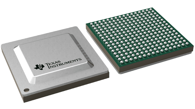
Packaging information
| Package | Pins FCBGA (ACF) | 256 |
| Operating temperature range (°C) -40 to 85 |
| Package qty | Carrier 90 | JEDEC TRAY (5+1) |
Features for the ADC12DL3200
- ADC Core:
- 12-Bit Resolution
- Up to 6.4 GSPS in Single-Channel Mode
- Up to 3.2 GSPS in Dual-Channel Mode
- Internal Dither for Low-Magnitude, High-Order Harmonics
- Low-Latency LVDS Interface:
- Total Latency: < 10 ns
- Up to 48 Data Pairs at 1.6 Gbps
- Four DDR Data Clocks
- Strobe Signals Simplify Synchronization
- Noise Floor (No Input, V FS = 1.0 V PP-DIFF):
- Dual-Channel Mode: –151.1 dBFS/Hz
- Single-Channel Mode: –154.3 dBFS/Hz
- Buffered Analog Inputs With V CMI of 0 V:
- Analog Input Bandwidth (–3 dB): 8.0 GHz
- Usable Input Frequency Range: > 10 GHz
- Full-Scale Input Voltage (V FS, Default): 0.8 V PP
- Noiseless Aperture Delay (T AD) Adjustment:
- Precise Sampling Control: 19-fs Step
- Simplifies Synchronization and Interleaving
- Temperature and Voltage Invariant Delays
- Easy-to-Use Synchronization Features:
- Automatic SYSREF Timing Calibration
- Timestamp for Sample Marking
- Power Consumption: 3.15 W
Description for the ADC12DL3200
The ADC12DL3200 is an RF-sampling, giga-sample, analog-to-digital converter (ADC) that can directly sample input frequencies from DC to above 10 GHz. In dual-channel mode, the ADC12DL3200 can sample up to 3200 MSPS and in single-channel mode up to 6400 MSPS. Programmable tradeoffs in channel count (dual-channel mode) and Nyquist bandwidth (single-channel mode) allow development of flexible hardware that meets the needs of both high-channel count or wide instantaneous signal bandwidth applications. Full-power input bandwidth (–3 dB) of 8.0 GHz and a useable frequency range allows direct RF sampling of L-band, S-band, C-band, and X-band for frequency agile systems.
The ADC12DL3200 uses a low-latency, low-voltage differential signaling (LVDS) interface for latency sensitive applications or when the simplicity of LVDS is preferred. The interface uses up to 48 data pairs, four double data rate (DDR) clocks, and four strobe signals arranged in four 12-bit data buses. The interface supports signaling rates of up to 1.6 Gbps. Strobe signals simplify synchronization across buses and between multiple devices. The strobe is generated internally and can be reset at a deterministic time by the SYSREF input. Multi-device synchronization is further eased by innovative synchronization features such as noiseless aperture delay (T AD) adjustment and SYSREF windowing.