Packaging information
| Package | Pins NFBGA (ZZE) | 198 |
| Operating temperature range (°C) -40 to 85 |
| Package qty | Carrier 160 | JEDEC TRAY (5+1) |
Features for the ADS52J90
- 16-Channel ADC Configurable to Convert
8, 16, or 32 Inputs - 10-, 12-, and 14-Bit Resolution Modes
- Maximum ADC Conversion Rate:
- 100 MSPS in 10-Bit Mode
- 80 MSPS in 12-Bit Mode
- 65 MSPS in 14-Bit Mode
- 16 ADCs Configurable to Convert:
- 8 Inputs with a Sampling Rate of a
2X ADC Conversion Rate - 16 Inputs with a Sampling Rate of a
1X ADC Conversion Rate - 32 Inputs with a Sampling Rate of a
0.5X ADC Conversion Rate
- 8 Inputs with a Sampling Rate of a
- LVDS Outputs with 16X, 14X, 12X, and 10X Serialization
- 5-Gbps JESD Interface:
- Supported in 16-Input and 32-Input Modes
- JESD204B Subclass 0, 1, and 2
- 2, 4, or 8 Channels per JESD Lane
- Optional Digital I-Q Demodulator (1)
- Supplies: 1.2 V, 1.8 V
- 2-VPP Differential Input, 0.8-V Common-Mode
- Differential or Single-Ended Input Clock
- Signal-to-Noise Ratio (SNR):
- 61 dBFS in 10-Bit Mode
- 70 dBFS in 12-Bit Mode
- 73.5 dBFS in 14-Bit Mode
- Power at 100 MSPS: 41 mW/Channel
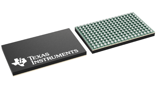
- Package: NFBGA-198 (9 mm × 15 mm)
- Pb-Free (RoHS Compliant) and Green
(1)Not detailed in this document. For details and information, contact factory.
Description for the ADS52J90
The ADS52J90 is a low-power, high-performance, 16-channel, analog-to-digital converter (ADC). The conversion rate of each ADC goes up to a maximum of 100 MSPS in 10-bit mode. The maximum conversion rate reduces when the ADC resolution is set to a higher value.
The device can be configured to accept 8, 16, or 32 inputs. In 32-input mode, each ADC alternately samples and converts two different inputs each at an effective sampling rate that is half of the ADC conversion rate. In 8-bit input mode, two ADCs convert the same input in an interleaved manner, resulting in an effective sampling rate that is twice the ADC conversion rate. The ADC is designed to scale its power with the conversion rate.
The ADC outputs are serialized and output through a low-voltage differential signaling (LVDS) interface along with a frame clock and a high-speed bit clock
The device also has an optional JESD204B interface while operating in the 16-input and 32-input modes. This interface runs up to 5 Gbps.
The ADS52J90 is available in a 9-mm × 15-mm, 0.8-mm pitch, NFBGA-198 package and is specified over a temperature range of –40°C to +85°C.