Features for the ADS58J89EVM
- Flexible input clock buffer with 1/2/4 divider to simplify clocking
- On chip dither to improve SFDR
- JESD204B data interface to simplify digital interface, compliant up to 5.0Gbps lane rates
- Supports JESD204B subclass 1 for synchronization and compatibility
- Channels A and B can be configured separately from channels C and D for mixed mode use
- Operating modes include 2x-decimation filter, SNRBoost, and triggered high-resolution burst data
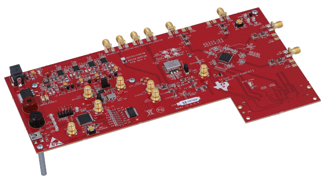
Description for the ADS58J89EVM
The ADS58J89 EVM demonstrates the performance of a quad 500Msps Receiver and Feedback IC with the JESD204B interface. It includes the ADS58J89 device, and JESD204B clocking is provided by the LMK04828 and TI voltage regulators to provide the necessary voltages. The input for each channel of the ADC is by default connected to a transformer input circuit which can be connected to a 50 ohm single ended signal source. The clock reference input is provided via a transformer input and can be connected to a 50 ohm single ended clock source. An onboard LMK04828 can be used to generate the necessary JESD204B clocks. Register access is provided through the on board USB connection and a GUI. An industry standard JESD204B pin assignment on an FMC connector allows direct connection to the TSW14J56 Capture Card as well as many commercially available FPGA development platforms.