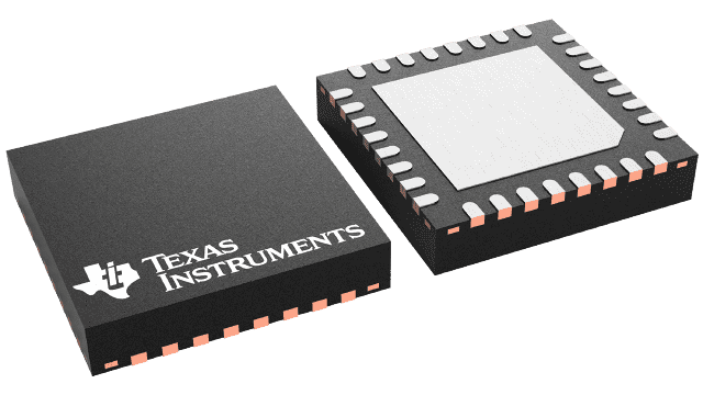
Packaging information
| Package | Pins VQFN (RHB) | 32 |
| Operating temperature range (°C) -40 to 125 |
| Package qty | Carrier 3,000 | LARGE T&R |
Features for the ADS8168
- Compact low-power data acquisition
system:
- MUX breakout enables single external driver amplifier
- 16-bit SAR ADC
- Low-drift integrated reference and buffer
- 0.5 × VREF output for analog input DC biasing
- Excellent AC and DC
performance:
- SNR: 92 dB, THD: –110 dB
- INL: ±0.3 LSB, 16-bit no missing codes
-
Multiplexer with channel sequencer:
- Multiple channel-sequencing options:
- Manual mode, on-the-fly mode, auto sequence mode, custom channel sequencing
- Early switching enables direct sensor interface
- Fast response time with on-the-fly mode
- Multiple channel-sequencing options:
- System
monitoring features:
- Per channel programmable window comparator
- False trigger avoidance with programmable hysteresis
- Enhanced-SPI digital interface:
- 1-MSPS throughput with 16-MHz SCLK
- High-speed, 70-MHz digital interface
- Wide operating range:
- External VREF input range: 2.5 V to 5 V
- AVDD from 3 V to 5.5 V
- DVDD from 1.65 V to 5.5 V
- –40°C to +125°C temperature range
Description for the ADS8168
The ADS816x is a
family of 16-bit, 8-channel, high-precision successive
approximation register (SAR) analog-to-digital converters (ADCs) operating from a single 5-V supply
with a 1-MSPS (ADS8168),
500-kSPS (ADS8167), and 250-kSPS (ADS8166) total throughput.
The input multiplexer supports extended settling time, which makes driving the analog inputs easier. The output of the multiplexer and ADC analog inputs are available as device pins. This configuration allows one ADC driver op amp to be used for all eight analog inputs of the multiplexer.
The ADS816x features a digital window comparator with programmable high and low alarm thresholds per analog input channel. The single op-amp solution with programmable alarm thresholds enables low power, low cost, and smallest form-factor applications.