Features for the CDCLVD1213EVM
- Easy-to-use evaluation board to fan out low-phase noise clocks
- Easy device setup
- Fast configuration
- Control pin configurable through jumpers
- Board powered at 2.5 V
- Differential input clocks
- Device and EVM support four LVDS outputs
Description for the CDCLVD1213EVM
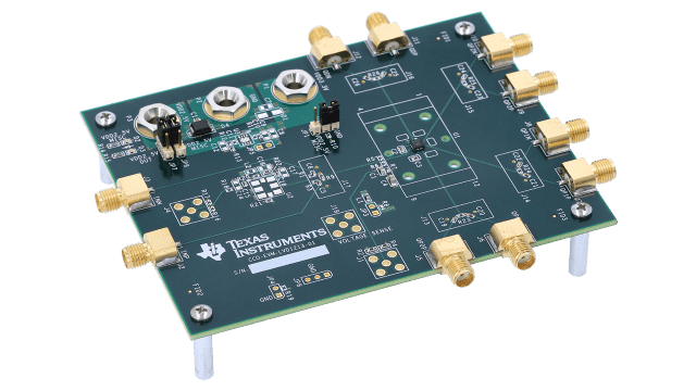
The CDCLVD1213 is a high-performance, low-additive jitter clock buffer with divider. The device has one differential input with internal 140-ohm differential input termination. The evaluation module (EVM) is designed to demonstrate the electrical performance of the CDCLVD1213. This fully assembled and factory-tested evaluation board allows complete validation of device functionalities. For optimum performance, the board is equipped with SMA connectors and well-controlled 50-ohm impedance microstrip transmission lines.