Features for the CDCLVP1216EVM
- 2:16 LVPECL Differential Buffer
- Selectable Clock Inputs Through Control Pin
- Universal Inputs Accept LVPECL, LVDS, and LVCMOS/LVTTL
- Maximum Clock Frequency: 2 GHz
- Maximum Core Current Consumption: 110mA
- Very Low Additive Jitter: < 100 fs,rms in 10 kHz to 20 MHz Offset Range
- 2.375 V to 3.6 V Device Power Supply
- Maximum Propagation Delay: 550 ps
- Maximum Output Skew: 30 ps
- Industrial Temperature Range: -40°C to +85°C
- ESD Protection Exceeds 2 kV (HBM
- Available in 7-mm X 7-mm QFN-48 (RGZ) Package
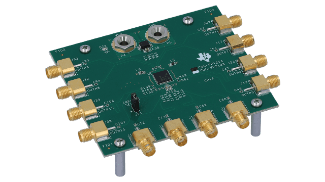
Description for the CDCLVP1216EVM
CDCLVP1216EVM is the evaluation module for CDCLVP1216. The CDCLVP1216 is a highly versatile, low additive jitter buffer that can generate 16 copies of LVPECL clock outputs from one of two selectable LVPECL, LVDS, or LVCMOS inputs. It has a maximum clock frequency up to 2 GHz. The overall additive jitter performance is less than 0.1 ps, RMS from 10 kHz to 20 MHz, and overall output skew is as low as 30 ps, making the device a perfect choice for use in demanding applications.