Features for the CDCM9102EVM
- Easy-to-use evaluation module to generate clock signals with low jitter and phase noise
- Easy device setup
- Control pins configurable through jumpers
- Requires 3.3-V power supply
- Single-ended or crystal input clock reference
- Termination available for LVPECL, LVDS, and LVCMOS output clocks
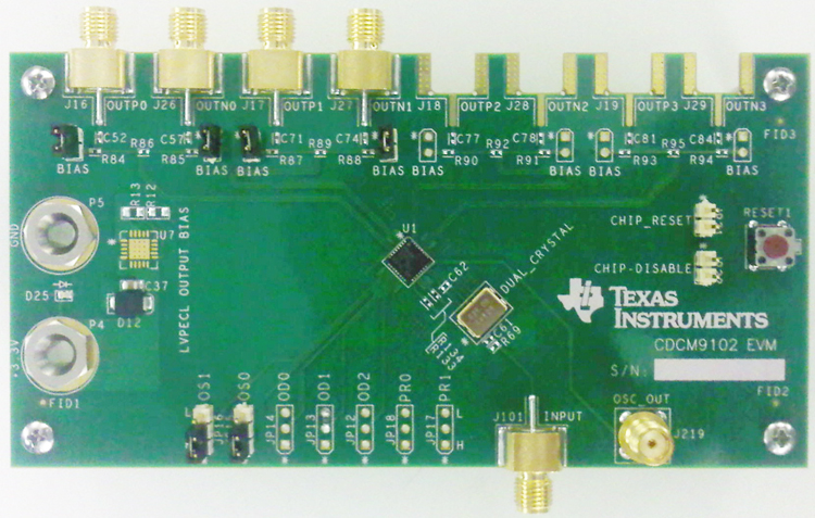
Description for the CDCM9102EVM
CDCM9102EVM is the evaluation module for CDCM9102, a low-jitter clock generator designed to provide reference clocks for communications standards such as PCI Express. The device is easy to configure and use. The CDCM9102 provides two 100-MHz differential clock ports. The output types supported for these ports include LVPECL, LVDS, or a pair of LVCMOS buffers. HCSL signaling is supported using an ac-coupled network. The user configures the output buffer type desired by strapping device pins. Additionally, a single-ended 25-MHz clock output port is provided. Uses for this port include general-purpose clocking, clocking Ethernet PHYs, or providing a reference clock for additional clock generators. All clocks generated are derived from a single external 25-MHz crystal. This fully-assembled and factory-tested evaluation board allows complete validation of all device functions.