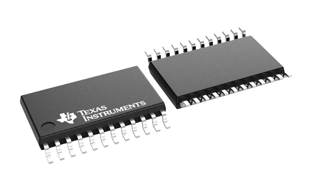
24-pin (PW) package image

CDCVF2310PWR ACTIVE

High performance 1:10 clock buffer for general purpose applications with support up to 105C

ACTIVE custom-reels CUSTOM Custom reel may be available
Same as: CDCVF2310PWRG4 This part number is identical to the part number listed above. You can only order quantities of the part number listed above.

Pricing

Qty Price
+

Additional package qty | Carrier options These products are exactly the same but come in a different carrier type

CDCVF2310PW ACTIVE
Package qty | Carrier 60 | TUBE
Inventory
Qty | Price 1ku | +

Quality information

Rating Catalog
RoHS Yes
REACH Yes
Lead finish / Ball material NIPDAU
MSL rating / Peak reflow Level-1-260C-UNLIM
Quality, reliability
& packaging information

Information included:

  • RoHS
  • REACH
  • Device marking
  • Lead finish / Ball material
  • MSL rating / Peak reflow
  • MTBF/FIT estimates
  • Material content
  • Qualification summary
  • Ongoing reliability monitoring
View or download
Additional manufacturing information

Information included:

  • Fab location
  • Assembly location
View

Export classification

*For reference only

  • US ECCN: EAR99

Packaging information

Package | Pins TSSOP (PW) | 24
Operating temperature range (°C) -40 to 85
Package qty | Carrier 2,000 | LARGE T&R

Features for the CDCVF2310

  • High-Performance 1:10 Clock Driver
  • Operates up to 200 MHz at VDD 3.3 V
  • Pin-to-Pin Skew < 100 ps at VDD 3.3 V
  • VDD Range: 2.3 V to 3.6 V
  • Operating Temperature Range –40°C to 105°C
  • Supports 105ºC Ambient Temperature (see
    Thermal Considerations)
  • Output Enable Glitch Suppression
  • Distributes One Clock Input to Two Banks of Five
    Outputs
  • 25-Ω On-Chip Series Damping Resistors
  • Packaged in 24-Pin TSSOP

Description for the CDCVF2310

The CDCVF2310 device is a high-performance, low-skew clock buffer that operates up to 200 MHz. Two banks of five outputs each provide low-skew copies of CLK. After power up, the default state of the outputs is low regardless of the state of the control pins. For normal operation, the outputs of bank 1Y[0:4] or 2Y[0:4] can be placed in a low state when the control pins (1G or 2G, respectively) are held low and a negative clock edge is detected on the CLK input. The outputs of bank 1Y[0:4] or 2Y[0:4] can be switched into the buffer mode when the control pins (1G and 2G) are held high and a negative clock edge is detected on the CLK input. The device operates in a 2.5-V and 3.3-V environment. The built-in output enable glitch suppression ensures a synchronized output enable sequence to distribute full period clock signals.

The CDCVF2310 is characterized for operation from –40°C to 85°C.
Pricing

Qty Price
+

Additional package qty | Carrier options These products are exactly the same but come in a different carrier type

CDCVF2310PW ACTIVE
Package qty | Carrier 60 | TUBE
Inventory
Qty | Price 1ku | +

Carrier options

You can choose different carrier options based on the quantity of parts, including full reel, custom reel, cut tape, tube or tray.

A custom reel is a continuous length of cut tape from one reel to maintain lot- and date-code traceability, built to the exact quantity requested. Following industry standards, a brass shim connects an 18-inch leader and trailer on both sides of the cut tape for direct feeding into automated assembly machines. TI includes a reeling fee for custom reel orders.

Cut tape is a length of tape cut from a reel. TI may fulfill orders using multiple strips of cut tapes or boxes to satisfy the quantity requested.

TI often ships tube or tray devices inside a box or in the tube or tray, depending on inventory availability. We pack all tapes, tubes or sample boxes according to internal electrostatic discharge and moisture-sensitivity-level protection requirements.

Learn more

Lot and date code selection may be available

Add a quantity to your cart and begin the checkout process to view the options available to select lot or date codes from existing inventory.

Learn more