Packaging information
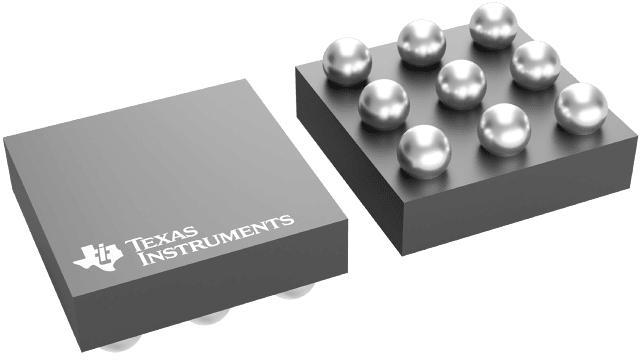
| Package | Pins DSBGA (YZF) | 9 |
| Operating temperature range (°C) -55 to 150 |
| Package qty | Carrier 3,000 | LARGE T&R |
Features for the CSD75207W15
- Dual P-Channel MOSFETs
- Common Source Configuration
- Small Footprint 1.5-mm × 1.5-mm
- Gate-Source Voltage Clamp
- Gate ESD Protection >4 kV
- HBM JEDEC standard JESD22-A114
- Pb and Halogen Free
- RoHS Compliant
Description for the CSD75207W15
The CSD75207W15 device is designed to deliver the lowest on-resistance and gate charge in the smallest outline possible with excellent thermal characteristics in an ultra-low profile. Low on-resistance coupled with the small footprint and low profile make the device ideal for battery-operated space-constrained applications. The device has also been awarded with U.S. patents 7952145, 7420247, 7235845, and 6600182.