Packaging information
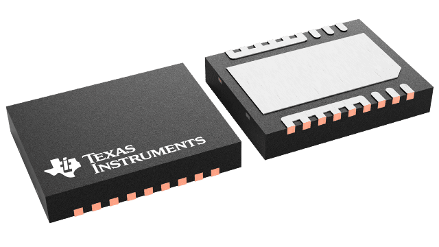
| Package | Pins VSON-CLIP (DPC) | 8 |
| Operating temperature range (°C) -40 to 150 |
| Package qty | Carrier 250 | SMALL T&R |
Features for the CSD97396Q4M
- Over 93% System Efficiency at 15 A
- Max Rated Continuous Current 30 A, Peak 65 A
- High Frequency Operation (up to 2 MHz)
- High Density – SON 3.5 mm × 4.5 mm Footprint
- Ultra-Low Inductance Package
- System-Optimized PCB Footprint
- Ultra-Low Quiescent (ULQ) Current Mode
- 3.3 V and 5 V PWM Signal Compatible
- Diode Emulation Mode With FCCM
- Input Voltages up to 24 V
- Tri-State PWM Input
- Integrated Bootstrap Diode
- Shoot-Through Protection
- RoHS Compliant – Lead Free Terminal Plating
- Halogen Free
Description for the CSD97396Q4M
The CSD97396Q4M NexFET Power Stage is a highly optimized design for use in a high-power, high-density synchronous buck converter. This product integrates the driver IC and NexFET technology to complete the power stage switching function. The driver IC has a built-in selectable diode emulation function that enables DCM operation to improve light load efficiency. In addition, the driver IC supports ULQ mode that enables connected standby for Windows 8. With the PWM input in tri-state, quiescent current is reduced to 130 µA, with immediate response. When SKIP# is held at tri-state, the current is reduced to 8 µA (typically 20 µs is required to resume switching). This combination produces a high current, high efficiency, and high speed switching device in a small 3.5 × 4.5 mm outline package. In addition, the PCB footprint is optimized to help reduce design time and simplify the completion of the overall system design.