Features for the LMK03318EVM
- High-performance PLL with 6 output dividers for clocking multiple interface standards/protocols
- Up to 8 pairs of Differential or 16 LVCMOS (1.8V) clock outputs, or any combination of both
- Flexible device pin modes offer multiple start-up register configurations (jumper selectable)
- Clock frequency margining: ±50 ppm adjustment of output frequencies via on-board pullable crystal
- GUI platform for full access to LMK03318 registers and EEPROM
Description for the LMK03318EVM
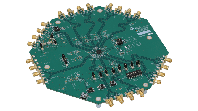
The LMK03318EVM evaluation module provides a complete clocking platform to evaluate the 100-fs RMS jitter performance and pin-/software-configuration modes and features of the Texas Instruments LMK03318 Ultra-Low-Jitter Clock Generator with 1 PLL, 8 outputs, 2 inputs, and integrated EEPROM.
The LMK03318EVM can be used as a flexible, multiple-output clock source for compliance testing, performance evaluation, and initial system prototyping. The edge-launch SMA ports provide access to the LMK03318 clock inputs and outputs for interfacing to test equipment and reference boards using commercially available coaxial cables, adapters, or baluns (not included). This connectivity enables integrated system level testing between TI’s LMK03318 and third-party FPGA/ASIC/SoC reference boards. A software graphical user interface (GUI) platform can be installed on a Host PC to access the LMK03318 device registers and EEPROM via the on-board USB-to-I2C interface. The GUI platform can also be used to export / import Register and EEPROM data files to facilitate factory or in-system programming of custom device configurations.