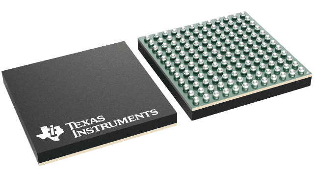
Packaging information
| Package | Pins NFBGA (ZCR) | 144 |
| Operating temperature range (°C) -40 to 85 |
| Package qty | Carrier 1,000 | LARGE T&R |
Features for the LMK04616
- Dual-loop PLL architecture
- Ultra low noise (10 kHz
to 20 MHz):
- 48-fs RMS jitter at 1966.08 MHz
- 50-fs RMS jitter at 983.04 MHz
- 61-fs RMS jitter at 122.88 MHz
- –165-dBc/Hz noise floor at 122.88 MHz
- JESD204B support
- Single shot, pulsed, and continuous SYSREF
-
16 differential output clocks in 8 frequency groups
- Programmable output swing between 700 mVpp to 1600 mVpp
- Each output pair can be configured to SYSREF clock output
- 16-bit channel divider
- Minimum SYSREF frequency of 25 kHz
- Maximum output frequency of 2 GHz
- Precision digital delay, dynamically adjustable
- Digital delay (DDLY) of ½ × clock distribution path frequency (2 GHz maximum)
- 60-ps step analog delay
- 50% duty cycle output divides, 1 to 65535
(even and odd)
- Four reference inputs
- Holdover mode, when inputs are lost
- Automatic and manual switch-over modes
- Loss-of-signal (LOS) detection
- 1.05-W typical power consumption with 16 outputs active
- Operates typically from a 1.8-V (outputs, inputs) and 3.3-V supply (digital, PLL1, PLL2_OSC, PLL2 core)
- Fully integrated programmable loop filter
- PLL2
- PLL2 phase detector rate up to 250 MHz
- OSCin frequency-doubler
- Integrated low-noise VCO
- Internal power conditioning: better than –80 dBc PSRR on VDDO for 122.88-MHz differential outputs
- 3- or 4-wire SPI interface (4-wire is default)
- –40ºC to +85ºC industrial ambient temperature
- Supports 105ºC PCB temperature (measured at thermal pad)
- LMK04616: 10-mm × 10-mm NFBGA-144 package with 0.8-mm pitch
Description for the LMK04616
The LMK0461x device family is the industry’s highest performance and lowest power jitter cleaner with JESD204B support. The 16 clock outputs can be configured to drive eight JESD204B converters or other logic devices using device and SYSREF clocks. The 17th output can be configured to provide a signal from PLL2 or a copy from the external VCXO.
Features like fully integrated PLL1 and PLL2 loop filters, a high number of integrated LDOs, digital and analog delay, the flexibility to supply outputs with 3.3V, 2.5V and 1.8V as well as the option to generate multiple SYSREF domains simultaneously makes the device easy to use.
Not limited to JESD204B applications each of the 17 outputs can be configured for traditional clocking systems.