Packaging information
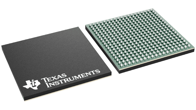
| Package | Pins NFBGA (GWT) | 361 |
| Operating temperature range (°C) -55 to 125 |
| Package qty | Carrier 90 | JEDEC TRAY (5+1) |
Features for the OMAPL138B-EP
- Highlights
- Dual Core SoC
- 345-MHz ARM926EJ-S™ RISC MPU
- 345-MHz C674x Fixed/Floating-Point VLIW DSP
- Supports TI’s Basic Secure Boot
- Enhanced Direct-Memory-Access Controller (EDMA3)
- Serial ATA (SATA) Controller
- DDR2/Mobile DDR Memory Controller
- Two Multimedia Card (MMC)/Secure Digital (SD) Card Interface
- LCD Controller
- Video Port Interface (VPIF)
- 10/100 Mb/s Ethernet MAC (EMAC)
- Programmable Real-Time Unit Subsystem
- Three Configurable UART Modules
- USB 1.1 OHCI (Host) With Integrated PHY
- One Multichannel Audio Serial Port
- Two Multichannel Buffered Serial Ports
- Dual Core SoC
- Dual Core SoC
- 345-MHz ARM926EJ-S™ RISC MPU
- 345-MHz C674x Fixed/Floating-Point VLIW DSP
- ARM926EJ-S Core
- 32-Bit and 16-Bit (Thumb®) Instructions
- DSP Instruction Extensions
- Single Cycle MAC
- ARM® Jazelle® Technology
- EmbeddedICE-RT™ for Real-Time Debug
- ARM9 Memory Architecture
- 16K-Byte Instruction Cache
- 16K-Byte Data Cache
- 8K-Byte RAM (Vector Table)
- 64K-Byte ROM
- C674x™ Instruction Set Features
- Superset of the C67x+™ and C64x+™ ISAs
- Up to 3648/2746 C674x MIPS/MFLOPS
- Byte-Addressable (8-/16-/32-/64-Bit Data)
- 8-Bit Overflow Protection
- Bit-Field Extract, Set, Clear
- Normalization, Saturation, Bit-Counting
- Compact 16-Bit Instructions
- C674x Two Level Cache Memory Architecture
- 32K-Byte L1P Program RAM/Cache
- 32K-Byte L1D Data RAM/Cache
- 256K-Byte L2 Unified Mapped RAM/Cache
- Flexible RAM/Cache Partition (L1 and L2)
- Enhanced Direct-Memory-Access Controller 3 (EDMA3):
- 2 Channel Controllers
- 3 Transfer Controllers
- 64 Independent DMA Channels
- 16 Quick DMA Channels
- Programmable Transfer Burst Size
- TMS320C674x Floating-Point VLIW DSP Core
- Load-Store Architecture With Non-Aligned Support
- 64 General-Purpose Registers (32 Bit)
- Six ALU (32-/40-Bit) Functional Units
- Supports 32-Bit Integer, SP (IEEE Single Precision/32-Bit)
and DP (IEEE Double Precision/64-Bit) Floating Point - Supports up to Four SP Additions Per Clock, Four DP
Additions Every 2 Clocks - Supports up to Two Floating Point (SP or DP)
Reciprocal Approximation (RCPxP) and Square-Root Reciprocal
Approximation (RSQRxP) Operations Per Cycle
- Supports 32-Bit Integer, SP (IEEE Single Precision/32-Bit)
- Two Multiply Functional Units
- Mixed-Precision IEEE Floating Point
Multiply Supported up to:- 2 SP x SP → SP Per Clock
- 2 SP x SP → DP Every Two Clocks
- 2 SP x DP → DP Every Three Clocks
- 2 DP x DP → DP Every Four Clocks
- Fixed Point Multiply Supports Two 32 × 32-Bit Multiplies,
Four 16 × 16-Bit Multiplies, or Eight 8 × 8-Bit
Multiplies per Clock Cycle, and Complex Multiples
- Mixed-Precision IEEE Floating Point
- Instruction Packing Reduces Code Size
- All Instructions Conditional
- Hardware Support for Modulo Loop Operation
- Protected Mode Operation
- Exceptions Support for Error Detection and Program Redirection
- Software Support
- TI DSP/BIOS™
- Chip Support Library and DSP Library
- 128K-Byte RAM Shared Memory
- 1.8V or 3.3V LVCMOS IOs (except for USB and DDR2 interfaces)
- Two External Memory Interfaces:
- EMIFA
- NOR (8-/16-Bit-Wide Data)
- NAND (8-/16-Bit-Wide Data)
- 16-Bit SDRAM With 128 MB Address Space
- DDR2/Mobile DDR Memory Controller
- 16-Bit DDR2 SDRAM With 512 MB Address Space or
- 16-Bit mDDR SDRAM With 256 MB Address Space
- Three Configurable 16550 type UART Modules:
- With Modem Control Signals
- 16-byte FIFO
- 16x or 13x Oversampling Option
- LCD Controller
- Two Serial Peripheral Interfaces (SPI) Each With Multiple Chip-Selects
- Two Multimedia Card (MMC)/Secure Digital (SD) Card Interface with
Secure Data I/O (SDIO) Interfaces - Two Master/Slave Inter-Integrated Circuit (I2C Bus™)
- One Host-Port Interface (HPI) With 16-Bit-Wide Muxed Address/Data Bus
For High Bandwidth - Programmable Real-Time Unit Subsystem (PRUSS)
- Two Independent Programmable Realtime Unit (PRU) Cores
- 32-Bit Load/Store RISC architecture
- 4K Byte instruction RAM per core
- 512 Bytes data RAM per core
- PRU Subsystem (PRUSS) can be disabled via software to save power
- Register 30 of each PRU is exported from the subsystem in addition to the
normal R31 output of the PRU cores.
- Standard power management mechanism
- Clock gating
- Entire subsystem under a single PSC clock gating domain
- Dedicated interrupt controller
- Dedicated switched central resource
- Two Independent Programmable Realtime Unit (PRU) Cores
- USB 1.1 OHCI (Host) With Integrated PHY (USB1)
- USB 2.0 OTG Port With Integrated PHY (USB0)
- USB 2.0 High-/Full-Speed Client
- USB 2.0 High-/Full-/Low-Speed Host
- End Point 0 (Control)
- End Points 1,2,3,4 (Control, Bulk, Interrupt or ISOC) Rx and Tx
- One Multichannel Audio Serial Port:
- Two Clock Zones and 16 Serial Data Pins
- Supports TDM, I2S, and Similar Formats
- DIT-Capable
- FIFO buffers for Transmit and Receive
- Two Multichannel Buffered Serial Ports:
- Supports TDM, I2S, and Similar Formats
- AC97 Audio Codec Interface
- Telecom Interfaces (ST-Bus, H100)
- 128-channel TDM
- FIFO buffers for Transmit and Receive
- 10/100 Mb/s Ethernet MAC (EMAC):
- IEEE 802.3 Compliant
- MII Media Independent Interface
- RMII Reduced Media Independent Interface
- Management Data I/O (MDIO) Module
- Video Port Interface (VPIF):
- Two 8-bit SD (BT.656), Single 16-bit or Single Raw (8-/10-/12-bit)
Video Capture Channels - Two 8-bit SD (BT.656), Single 16-bit Video Display Channels
- Two 8-bit SD (BT.656), Single 16-bit or Single Raw (8-/10-/12-bit)
- Universal Parallel Port (uPP):
- High-Speed Parallel Interface to FPGAs and Data Converters
- Data Width on Each of Two Channels is 8- to 16-bit Inclusive
- Single Data Rate or Dual Data Rate Transfers
- Supports Multiple Interfaces with START, ENABLE and WAIT Controls
- Serial ATA (SATA) Controller:
- Supports SATA I (1.5 Gbps) and SATA II (3.0 Gbps)
- Supports all SATA Power Management Features
- Hardware-Assisted Native Command Queueing (NCQ) for up to 32 Entries
- Supports Port Multiplier and Command-Based Switching
- Real-Time Clock With 32 KHz Oscillator(1) and Separate Power Rail
- Three 64-Bit General-Purpose Timers (Each Configurable as Two 32-Bit Timers)
- One 64-bit General-Purpose/Watchdog Timer (Configurable as Two 32-bit General-Purpose Timers)
- Two Enhanced Pulse Width Modulators (eHRPWM):
- Dedicated 16-Bit Time-Base Counter With Period And Frequency Control
- 6 Single Edge, 6 Dual Edge Symmetric or 3 Dual Edge Asymmetric Outputs
- Dead-Band Generation
- PWM Chopping by High-Frequency Carrier
- Trip Zone Input
- Three 32-Bit Enhanced Capture Modules (eCAP):
- Configurable as 3 Capture Inputs or 3 Auxiliary Pulse Width Modulator (APWM) outputs
- Single Shot Capture of up to Four Event Time-Stamps
- 361-Ball SnPb Plastic Ball Grid Array (PBGA) [GWT Suffix], 0.80-mm Ball Pitch
- Available in Military (-55°C to 125°C) Temperature Range
Supports Defense, Aerospace, and Medical Applications
- Controlled Baseline
- One Assembly/Test Site
- One Fabrication Site
- Available in Extended (–55°C/125°C) Temperature Range
- Extended Product Life Cycle
- Extended Product-Change Notification
- Product Traceability
(1) Crystal oscillator cannot be operated beyond 105°C.
- EMIFA
Description for the OMAPL138B-EP
The OMAPL138B C6-Integra™ DSP+ARM® processor is a low-power applications processor based on an ARM926EJ-S™ and a C674x DSP core. It provides significantly lower power than other members of the TMS320C6000™ platform of DSPs.
The device enables OEMs and ODMs to quickly bring to market devices featuring robust operating systems support, rich user interfaces, and high processing performance life through the maximum flexibility of a fully integrated mixed processor solution.
The dual-core architecture of the device provides benefits of both DSP and Reduced Instruction Set Computer (RISC) technologies, incorporating a high-performance TMS320C674x DSP core and an ARM926EJ-S core.
The ARM926EJ-S is a 32-bit RISC processor core that performs 32-bit or 16-bit instructions and processes 32-bit, 16-bit, or 8-bit data. The core uses pipelining so that all parts of the processor and memory system can operate continuously.
The ARM core has a coprocessor 15 (CP15), protection module, and Data and program Memory Management Units (MMUs) with table look-aside buffers. It has separate 16K-byte instruction and 16K-byte data caches. Both are four-way associative with virtual index virtual tag (VIVT). The ARM core also has a 8KB RAM (Vector Table) and 64KB ROM.
The device DSP core uses a two-level cache-based architecture. The Level 1 program cache (L1P) is a 32KB direct mapped cache and the Level 1 data cache (L1D) is a 32KB 2-way set-associative cache. The Level 2 program cache (L2P) consists of a 256KB memory space that is shared between program and data space. L2 memory can be configured as mapped memory, cache, or combinations of the two. Although the DSP L2 is accessible by ARM and other hosts in the system, an additional 128KB RAM shared memory is available for use by other hosts without affecting DSP performance.
For security enabled devices, TI’s Basic Secure Boot allows users to protect proprietary intellectual property and prevents external entities from modifying user-developed algorithms. By starting from a hardware-based “root-of-trust”, the secure boot flow guarantees a known good starting point for code execution. By default, the JTAG port is locked down to prevent emulation and debug attacks but can be enabled during the secure boot process during application development. The boot modules themselves are encrypted while sitting in external non-volatile memory, such as flash or EEPROM, and are decrypted and authenticated when loaded during secure boot. This protects the users’ IP and enables them to securely set up the system and begin device operation with known, trusted code. Basic Secure Boot utilizes either SHA-1 or SHA-256, and AES-128 for boot image validation. It also uses AES-128 for boot image encryption. The secure boot flow employs a multi-layer encryption scheme which not only protects the boot process but offers the ability to securely upgrade boot and application software code. A 128-bit device-specific cipher key, known only to the device and generated using a NIST-800-22 certified random number generator, is used to protect user encryption keys. When an update is needed, the customer creates a new encrypted image using its encryption keys. Then the device can acquire the image via an external interface, such as Ethernet, and overwrite the existing code. For more details on the supported security features or TI’s Basic Secure Boot, refer to the TMS320C674x/OMAP-L1x Processor Security User’s Guide (SPRUGQ9).
The peripheral set includes: a 10/100 Mb/s Ethernet MAC (EMAC) with a Management Data Input/Output (MDIO) module; one USB2.0 OTG interface; one USB1.1 OHCI interface; two inter-integrated circuit (I2C) Bus interfaces; one multichannel audio serial port (McASP) with 16 serializers and FIFO buffers; two multichannel buffered serial ports (McBSP) with FIFO buffers; two SPI interfaces with multiple chip selects; four 64-bit general-purpose timers each configurable (one configurable as watchdog); a configurable 16-bit host port interface (HPI) ; up to 9 banks of 16 pins of general-purpose input/output (GPIO) with programmable interrupt/event generation modes, multiplexed with other peripherals; three UART interfaces (each with RTS and CTS); two enhanced high-resolution pulse width modulator (eHRPWM) peripherals; 3 32-bit enhanced capture (eCAP) module peripherals which can be configured as 3 capture inputs or 3 auxiliary pulse width modulator (APWM) outputs; and 2 external memory interfaces: an asynchronous and SDRAM external memory interface (EMIFA) for slower memories or peripherals, and a higher speed DDR2/Mobile DDR controller.
The Ethernet Media Access Controller (EMAC) provides an efficient interface between the device and a network. The EMAC supports both 10Base-T and 100Base-TX, or 10 Mbits/second (Mbps) and 100 Mbps in either half- or full-duplex mode. Additionally an Management Data Input/Output (MDIO) interface is available for PHY configuration. The EMAC supports both MII and RMII interfaces.
The SATA controller provides a high-speed interface to mass data storage devices. The SATA controller supports both SATA I (1.5 Gbps) and SATA II (3.0 Gbps).
The Universal Parallel Port (uPP) provides a high-speed interface to many types of data converters, FPGAs or other parallel devices. The UPP supports programmable data widths between 8- to 16-bits on each of two channels. Single-data rate and double-data rate transfers are supported as well as START, ENABLE and WAIT signals to provide control for a variety of data converters.
A Video Port Interface (VPIF) is included providing a flexible video input/output port.
The rich peripheral set provides the ability to control external peripheral devices and communicate with external processors. For details on each of the peripherals, see the related sections later in this document and the associated peripheral reference guides.
The device has a complete set of development tools for the ARM and DSP. These include C compilers, a DSP assembly optimizer to simplify programming and scheduling, and a Windows™ debugger interface for visibility into source code execution.