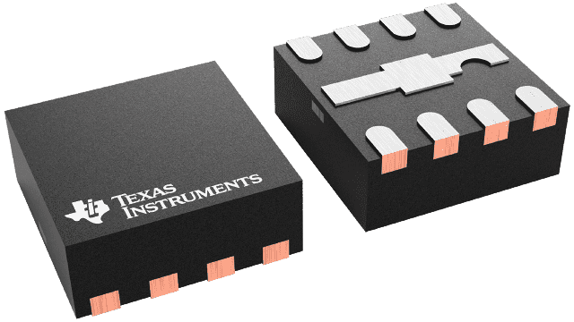
8-pin (DRF) package image

SN65LVDS17DRFR ACTIVE

2.5-V/3.3-V oscillator gain stage/buffer with enable

ACTIVE custom-reels CUSTOM Custom reel may be available

Pricing

Qty Price
+

Additional package qty | Carrier options These products are exactly the same but come in a different carrier type

SN65LVDS17DRFT ACTIVE custom-reels CUSTOM Custom reel may be available
Package qty | Carrier 250 | SMALL T&R
Inventory
Qty | Price 1ku | +

Quality information

Rating Catalog
RoHS Yes
REACH Yes
Lead finish / Ball material NIPDAU
MSL rating / Peak reflow Level-1-260C-UNLIM
Quality, reliability
& packaging information

Information included:

  • RoHS
  • REACH
  • Device marking
  • Lead finish / Ball material
  • MSL rating / Peak reflow
  • MTBF/FIT estimates
  • Material content
  • Qualification summary
  • Ongoing reliability monitoring
View or download
Additional manufacturing information

Information included:

  • Fab location
  • Assembly location
View

Export classification

*For reference only

  • US ECCN: EAR99

Packaging information

Package | Pins WSON (DRF) | 8
Operating temperature range (°C) -40 to 85
Package qty | Carrier 3,000 | LARGE T&R

Features for the SN65LVDS17

  • Low-Voltage PECL Input and Low-Voltage PECL or LVDS Outputs
  • Clock Rates to 2 GHz
    • 140-ps Output Transition Times
    • 0.11 ps Typical Intrinsic Phase Jitter
    • Less than 630 ps Propagation Delay Times
  • 2.5-V or 3.3-V Supply Operation
  • 2-mm × 2-mm Small-Outline No-Lead Package
  • APPLICATIONS
    • PECL-to-LVDS Translation
    • Clock Signal Amplification

Description for the SN65LVDS17

These four devices are high-frequency oscillator gain stages supporting both LVPECL or LVDS on the high gain outputs in 3.3-V or 2.5-V systems. Additionally, provides the option of both single-ended input (PECL levels on the SN65LVx16) and fully differential inputs on the SN65LVx17.

The SN65LVx16 provides the user a Gain Control (GC) for controlling the Q output from 300 mV to 860 mV either by leaving it open (NC), grounded, or tied to VCC. (When left open, the Q output defaults to 575 mV.) The Q on the SN65LVx17 defaults to 575 mV as well.

Both devices provide a voltage reference (VBB) of typically 1.35 V below VCC for use in receiving single-ended PECL input signals. When not used, VBB should be unconnected or open.

All devices are characterized for operation from -40°C to 85°C.
Pricing

Qty Price
+

Additional package qty | Carrier options These products are exactly the same but come in a different carrier type

SN65LVDS17DRFT ACTIVE custom-reels CUSTOM Custom reel may be available
Package qty | Carrier 250 | SMALL T&R
Inventory
Qty | Price 1ku | +

Carrier options

You can choose different carrier options based on the quantity of parts, including full reel, custom reel, cut tape, tube or tray.

A custom reel is a continuous length of cut tape from one reel to maintain lot- and date-code traceability, built to the exact quantity requested. Following industry standards, a brass shim connects an 18-inch leader and trailer on both sides of the cut tape for direct feeding into automated assembly machines. TI includes a reeling fee for custom reel orders.

Cut tape is a length of tape cut from a reel. TI may fulfill orders using multiple strips of cut tapes or boxes to satisfy the quantity requested.

TI often ships tube or tray devices inside a box or in the tube or tray, depending on inventory availability. We pack all tapes, tubes or sample boxes according to internal electrostatic discharge and moisture-sensitivity-level protection requirements.

Learn more

Lot and date code selection may be available

Add a quantity to your cart and begin the checkout process to view the options available to select lot or date codes from existing inventory.

Learn more