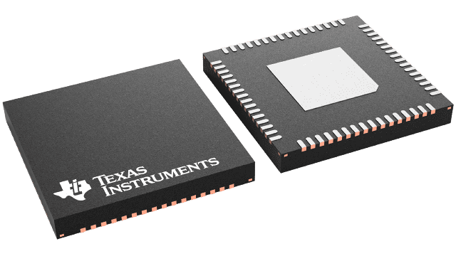
Packaging information
| Package | Pins VQFN (RSK) | 64 |
| Operating temperature range (°C) -40 to 85 |
| Package qty | Carrier 2,000 | LARGE T&R |
Features for the SN65LVDS314
- Serial Interface Technology
- Compatible with FlatLink3G such as SN65LVDS301 and SN65LVDS311
- Supports Video Interfaces up to 24-bit RGB Data and 3 Control Bits Received over
1, 2 or 3 SubLVDS Differential Lines - SubLVDS Differential Voltage Levels
- Flexible RGB Signaling Level of 1.8 V to 3.3 V
- Up to 1.755 Gbps Data Throughput
- Three Operating Modes to Conserve Power
- Active mode QVGA - 17 mW
- Typical Shutdown - 0.6 µW
- Typical Standby Mode - 54 µW Typical
- Bus-Swap Function for PCB-Layout Flexibility
- ESD Rating > 4 kV (HBM)
- Pixel Clock Range of 4 MHz–65 MHz
- Failsafe on all CMOS Inputs
- Packaged in 8 mm × 8 mm QFN with 0.4 mm pin pitch
- Very low EMI meets SAE J1752/3 'Kh'-spec
Description for the SN65LVDS314
The SN65LVDS314 receiver de-serializes FlatLink™3G compliant serial input data to 27 parallel data outputs. The SN65LVDS314 receiver contains one shift register to load 30 bits from 1, 2 or 3 serial inputs and latches the 24 pixel bits and 3 control bits out to the parallel CMOS outputs after checking the parity bit. If the parity check confirms correct parity, the Channel Parity Error (CPE) output remains low. If a parity error is detected, the CPE output generates a high pulse while the data output bus disregards the newly-received pixel. Instead, the last data word is held on the output bus for another clock cycle.
The serial data and clock are received via Sub Low-Voltage Differential Signalling (SubLVDS) lines. The SN65LVDS314 supports three operating power modes (Shutdown, Standby, and Active) to conserve power.
When receiving, the PLL locks to the incoming clock CLK and generates an internal high-speed clock at the line rate of the data lines. The data is serially loaded into a shift register using the internal high-speed clock. The deserialized data is presented on the parallel output bus with a recreation of the Pixel clock PCLK generated from the internal high-speed clock. If no input CLK signal is present, the output bus is held static with the PCLK and DE held low, while all other parallel outputs are pulled high.
The parallel (CMOS) output bus offers a bus-swap feature. The SWAP control pin controls the output pin order of the output pixel data to be either R[7:0]. G[7:0], B[7:0], VS, HS, DE or B[0:7], G[0:7], R[0:7], VS, HS, DE. This gives a PCB designer the flexibility to better match the bus to the LCD driver pinout or to put the receiver device on the top side or the bottom side of the PCB. The F/S control input selects between a slow CMOS bus output rise time for best EMI and power consumption and a fast CMOS output for increased speed or higher load designs.
Two Link Select lines LS0 and LS1 select whether 1, 2, or 3 serial links are used. The RXEN input may be used to put the SN65LVDS314 in a Shutdown mode. The SN65LVDS314 enters an active Standby mode if the common mode voltage of the CLK input becomes shifted to VDDLVDS (e.g., transmitter releases the CLK output into high-impedance). This minimizes power consumption without the need of switching an external control pin. The SN65LVDS314 is characterized for operation over ambient air temperatures of –40°C to 85°C. All CMOS and SubLVDS signals are 2-V tolerant with VDD = 0 V. This feature allows signal powerup before VDD is stabilized.
