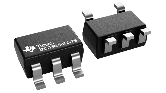
SN74LV1T34DCKR ACTIVE
Single Power Supply BUFFER Logic Level Shifter (no enable)
Quality information
RoHS | Yes |
---|---|
REACH | Yes |
Lead finish / Ball material | NIPDAU, SN |
MSL rating / Peak reflow | Level-1-260C-UNLIM |
Quality, reliability & packaging information Information included:
|
View or download |
More SN74LV1T34 information
Packaging information
Package | Pins | Package qty | Carrier: | Operating temperature range (°C) |
---|---|---|
SOT-SC70 (DCK) | 5 |
3,000 | LARGE T&R
Custom reel may be available |
-40 to 125 |
Package | Pins | SOT-SC70 (DCK) | 5 |
---|---|
Package qty | Carrier: |
3,000 | LARGE T&R
Custom reel may be available |
Operating temperature range (°C) | -40 to 125 |
Features for the SN74LV1T34
- Latch-Up Performance Exceeds 250 mA
Per JESD 17 - ESD Performance Tested Per JESD 22
- 2000-V Human-Body Model
(A114-B, Class II) - 200-V Machine Model (A115-A)
- 1000-V Charged-Device Model(C101)
- 2000-V Human-Body Model
- Single-Supply Voltage Translator at 5-V, 3.3-V, 2.5-V, and 1.8-V VCC
- Operating Range of 1.65 V to 5.5 V
- Up Translation
- 1.2 V(1) to 1.8 V at 1.8-VVCC
- 1.5 V(1) to 2.5 V at 2.5-VVCC
- 1.8 V(1) to 3.3 V at3.3-V VCC
- 3.3 V to 5.0 V at 5.0-VVCC
- Down Translation
- 3.3 V to 1.8 V at 1.8-V VCC
- 3.3 V to 2.5 V at 2.5-V VCC
- 5 V to3.3 V at 3.3-V VCC
- Logic Output is Referenced to VCC
- Output Drive
- 8 mA Output Drive at 5.0 V
- 7 mA Output Drive at 3.3 V
- 3 mA Output Drive at 1.8V
- Characterized up to 50 MHz at 3.3 V VCC
- 5-V Tolerance on Input Pins
- –40°C to +125°C Operating Temperature Range
- Supports Standard Logic Pinouts
- CMOS Output Backward Compatible With AUP1G and LVC1G Families (1)
(1)Refer to the VIH/VIL and output drive for lower VCC condition
All trademarks are the property of their respective owners.
Description for the SN74LV1T34
The SN74LV1T34 device is a low voltage CMOS gate logic that operates at a wider voltagerange for industrial, portable, and telecom applications. The output level is referenced to thesupply voltage and is able to support 1.8-V, 2.5-V, 3.3-V, and 5-V CMOS levels.
The input is designed with a lower threshold circuit to match 1.8 V input logic atVCC = 3.3 V and can be used in 1.8 V to 3.3 V level up translation. Inaddition, the 5 V tolerant input pins enable down translation (that is, 3.3 V to 2.5 V output atVCC = 2.5 V). The wide VCC range of 1.8 V to 5.5 Vallows generation of desired output levels to connect to controllers or processors.
The SN74LV1T34 device is designed with current-drive capability of 8 mA to reduce linereflections, overshoot, and undershoot caused by high-drive outputs.
Pricing
Qty | Price (USD) |
---|---|
1-99 | 0.201 |
100-249 | 0.137 |
250-999 | 0.105 |
1,000+ | 0.07 |