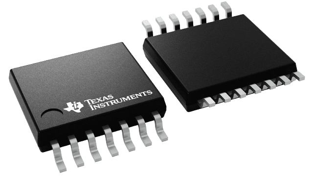
Packaging information
| Package | Pins TSSOP (PW) | 14 |
| Operating temperature range (°C) -40 to 125 |
| Package qty | Carrier 2,000 | LARGE T&R |
Features for the SN74LVC125A-Q1
- Qualified for automotive applications
- Operates from 1.65V to 3.6V
- Specified from –40°C to 125°C
- Inputs accept voltages to 5.5V
- Max tpd of 4.8ns at 3.3V
- Typical VOLP (output ground bounce) <0.8V at VCC = 3.3V, TA = 25°C
- Typical VOHV (output VOH undershoot) >2V at VCC = 3.3V, TA = 25°C
- Latch-up performance exceeds 250mA per JESD 17
Description for the SN74LVC125A-Q1
This quadruple bus buffer gate is designed for 1.65V to 3.6V VCC operation.