Packaging information
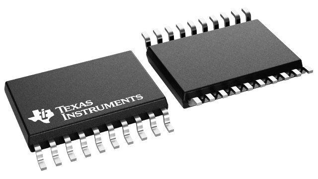
| Package | Pins TSSOP (PW) | 20 |
| Operating temperature range (°C) -40 to 125 |
| Package qty | Carrier 2,000 | LARGE T&R |
Features for the SN74LVC540A-Q1
- Qualified for Automotive Applications
- ESD Protection Exceeds 2000 V Per MIL-STD-883, Method 3015; Exceeds 200 V Using Machine Model (C = 200 pF, R = 0)
- Operates From 2 V to 3.6 V
- Inputs Accept Voltages to 5.5 V
- Max tpd of 5.3 ns at 3.3 V
- Typical VOLP (Output Ground Bounce)
<0.8 V at VCC = 3.3 V, TA = 25°C - Typical VOHV (Output VOH Undershoot)
>2 V at VCC = 3.3 V, TA = 25°C - Supports Mixed-Mode Signal Operation on All Ports (5-V Input/Output Voltage With 3.3-V VCC)
- Ioff Supports Partial-Power-Down Mode Operation
Description for the SN74LVC540A-Q1
The SN74LVC540A octal buffer/driver is designed for 2.7-V to 3.6-V VCC operation.
This device is ideal for driving bus lines or buffer-memory address registers. This device features inputs and outputs on opposite sides of the package that facilitate printed circuit board layout.
The 3-state control gate is a 2-input AND gate with active-low inputs so that, if either output-enable (OE1 or OE2) input is high, all outputs are in the high-impedance state.
Inputs can be driven from either 3.3-V or 5-V devices. This feature allows the use of this device as a translator in a mixed 3.3-V/5-V system environment.
This device is fully specified for partial-power-down applications using Ioff. The Ioff circuitry disables the outputs, preventing damaging current backflow through the device when it is powered down.
To ensure the high-impedance state during power up or power down, OE should be tied to VCC through a pullup resistor; the minimum value of the resistor is determined by the current-sinking capability of the driver.