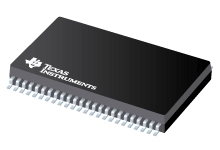
SN74SSTV16859RGQ8 image

SN74SSTV16859RGQ8 LAST TIME BUY

200-MHz, 13-bit to 26-bit registered buffer with SSTL_2 inputs and outputs

LAST TIME BUY custom-reels CUSTOM Custom reel may be available
open-in-new View alternates

Pricing

Qty Price
+

Quality information

Rating Military
RoHS Yes
REACH Yes
Lead finish / Ball material SN
MSL rating / Peak reflow Level-3-260C-168 HR
Quality, reliability
& packaging information

Information included:

  • RoHS
  • REACH
  • Device marking
  • Lead finish / Ball material
  • MSL rating / Peak reflow
  • MTBF/FIT estimates
  • Material content
  • Qualification summary
  • Ongoing reliability monitoring
View or download
Additional manufacturing information

Information included:

  • Fab location
  • Assembly location
View

Export classification

*For reference only

  • US ECCN: EAR99

Packaging information

Package | Pins VQFNP (RGQ) | 56
Operating temperature range (°C) 0 to 70
Package qty | Carrier 2,000 | LARGE T&R

Features for the SN74SSTV16859

  • Member of the Texas Instruments Widebus™ Family
  • 1-to-2 Outputs to Support Stacked DDR DIMMs
  • Supports SSTL_2 Data Inputs
  • Outputs Meet SSTL_2 Class II Specifications
  • Differential Clock (CLK and CLK\) Inputs
  • Supports LVCMOS Switching Levels on the RESET\ Input
  • RESET\ Input Disables Differential Input Receivers, Resets All Registers, and Forces All Outputs Low
  • Pinout Optimizes DIMM PCB Layout
  • Latch-Up Performance Exceeds 100 mA Per JESD 78, Class II
  • ESD Protection Exceeds JESD 22
    • 2000-V Human-Body Model (A114-A)
    • 200-V Machine Model (A115-A)

Widebus is a trademark of Texas Instruments.

Description for the SN74SSTV16859

This 13-bit to 26-bit registered buffer is designed for 2.3-V to 2.7-V VCC operation.

All inputs are SSTL_2, except the LVCMOS reset (RESET)\ input. All outputs are SSTL_2, Class II compatible.

The SN74SSTV16859 operates from a differential clock (CLK and CLK\). Data are registered at the crossing of CLK going high and CLK\ going low.

The device supports low-power standby operation. When RESET\ is low, the differential input receivers are disabled, and undriven (floating) data, clock, and reference voltage (VREF) inputs are allowed. In addition, when RESET\ is low, all registers are reset and all outputs are forced low. The LVCMOS RESET\ input always must be held at a valid logic high or low level.

To ensure defined outputs from the register before a stable clock has been supplied, RESET\ must be held in the low state during power up.
Pricing

Qty Price
+

Carrier options

You can choose different carrier options based on the quantity of parts, including full reel, custom reel, cut tape, tube or tray.

A custom reel is a continuous length of cut tape from one reel to maintain lot- and date-code traceability, built to the exact quantity requested. Following industry standards, a brass shim connects an 18-inch leader and trailer on both sides of the cut tape for direct feeding into automated assembly machines. TI includes a reeling fee for custom reel orders.

Cut tape is a length of tape cut from a reel. TI may fulfill orders using multiple strips of cut tapes or boxes to satisfy the quantity requested.

TI often ships tube or tray devices inside a box or in the tube or tray, depending on inventory availability. We pack all tapes, tubes or sample boxes according to internal electrostatic discharge and moisture-sensitivity-level protection requirements.

Learn more

Lot and date code selection may be available

Add a quantity to your cart and begin the checkout process to view the options available to select lot or date codes from existing inventory.

Learn more