Features for the TPS50601SPEVM-D
- Integrated 55-mΩ/50-mΩ MOSFETs
- Split Power Rail: 1.6 V to 6.3 V on PVIN
- Power Rail: 3 V to 6.3 V on VIN
- SEL Latchup Immune to LET = 85 MeV
- Total Dose (TID) tolerance = 100kRad (Si)
- 0.795-V ±1.258% Voltage Reference at 25°C
- Monotonic Start-Up into Pre-Biased Outputs
- Adjustable Slow Start and Power Sequencing
- Power Good Output Monitor for Undervoltage and Overvoltage
- Adjustable Input Undervoltage Lockout
- APPLICATIONS
- Point of Load Regulation
- TPS50601-SP: Rad Tolerant Applications
- Supports Harsh Environment Applications
- TPS50601-SP Available in Military (–55°C to 125°C) Temperature Range (1)
(1) Custom temperature ranges available
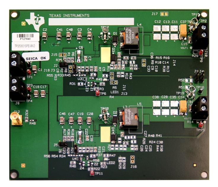
Description for the TPS50601SPEVM-D
The TPS50601-SP DC/DC converter is designed to provide up to a 6-A output in single phase operation (TPS50601SPEVM-S) and up to 12 A in dual phase operation (TPS50601SPEVM-D), when each phase is configured to provide 6-A per phase.
TPS50601SPEVM-D can also be configured such that each phase provides 3 A and, with current sharing between phase 1 and phase 2, a total of 6 A can be provided to meet system needs. This configuration will provide higher reliability (MTBF) for system needs due to reduced stresses on components and higher efficiency. The TPS50601SPEVM-D can also be configured to operate as two single output voltages; i.e. 2.5 V and 1.8 V each providing 6 A or a dual phase operation such that the two phases can be paralleled thus being capable of providing 12-A steady state load.
The TPS50601SPEVM implements split-input power rails with separate input voltage inputs for the power stage and control circuitry. The power stage input voltage (PVIN) is rated for 1.6 V to 6.3 V while the control input voltage (VIN) is rated for 3 V to 6.3 V. The TPS50601SPEVM provides both input voltages but it is designed and tested using the PVIN connected to VIN. Rated input voltage and output current ranges for the EVM are given in Table 1. This EVM is designed to demonstrate features of the TPS50601-SP, as well as to provide flexibility so that input/output capacitors and output inductors, as well as other components (such as frequency adjust range, output voltage and compensations components) can be modified when evaluating the TPS50601-SP converter using this EVM.
TPS50601-SP will operate with switching frequency of 100-kHz to 1-MHz range. For the EVM, 100 kHz was selected as it would provide higher efficiency. The high-side and low-side MOSFETs are incorporated inside the TPS50601-SP package along with the gate drive circuitry. The low drain-to-source on-resistance of the MOSFET allows the TPS50601-SP to achieve high efficiencies and helps keep the junction temperature low at high output currents. The compensation components are external to the integrated circuit (IC), and an external divider allows for an adjustable output voltage. Additionally, the TPS50601-SP provides adjustable slow start, tracking, and undervoltage lockout inputs.
Note: This EVM contains Pb, a necessary component for QML parts