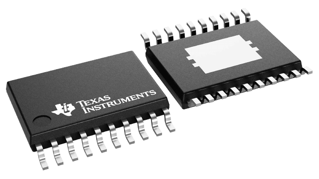
Packaging information
| Package | Pins HTSSOP (PWP) | 20 |
| Operating temperature range (°C) -40 to 125 |
| Package qty | Carrier 2,000 | LARGE T&R |
Features for the TPS55160-Q1
- Qualified for automotive applications
- AEC-Q100 qualified with the following results:
- Device temperature grade 1: –40°C to +125°C ambient operating temperature
- Device HBM ESD classification level 2
- Device CDM ESD classification level C4B
- Functional Safety-Capable
- 2-V to 36-V input voltage range for VOUT = 5 V
- 5-V or 12-V fixed output voltage (TPS55165-Q1)
- Adjustable output voltage options from 5.7 V to 9 V (TPS55160-Q1 and TPS55162-Q1)
- Up to 85% efficiency
- 1-A output current for VOUT = 5 V and VIN ≥ 5.3 V
- 0.8-A output current for VOUT = 5 V and VIN ≥ 3.8 V
- 0.4-A output current for VOUT = 5 V and VIN ≥ 2.3 V
- Automatic transition between step-down and step-up mode
- Low-power mode for improved efficiency at light load conditions (TPS55160-Q1/TPS55165-Q1)
- Device quiescent current less than 15 µA in low-power mode (TPS55160-Q1/TPS55165-Q1)
- Device shutdown current less than 3 µA
- Forced fixed-frequency operation at 2 MHz
- Selectable spread spectrum (TPS55160-Q1 and TPS55165-Q1)
- Wake-up through IGN with power-latch function
- Smart power-good output with configurable delay time
- Overtemperature protection and output overvoltage protection
- Available in easy-to-use 20-Pin HTSSOP PowerPAD™ package
Description for the TPS55160-Q1
The TPS5516x-Q1 family of devices is a high-voltage synchronous buck-boost DC-DC converter. The device provides a stable power-supply output from a wide varying input-power supply such as an automotive car battery. The buck-boost overlap control ensures automatic transition between step-down and step-up mode with optimal efficiency. The TPS55165-Q1 output voltage can be set to a fixed level of 5 V or 12 V. The TPS55160-Q1 and TPS55162-Q1 devices have a configurable output voltage ranging from 5.7 V to 9 V that is set by an external resistive divider.
Output currents can be as high as 1 A for a normal car battery voltage, and can be maintained at 0.4 A for lower input voltages, such as those for common battery-cranking profiles. The buck-boost converter is based on a fixed-frequency, pulse-width-modulation (PWM) control circuit using synchronous rectification to obtain maximum efficiency. The switching frequency is set to 2 MHz (typical) which allows for the usage of a small inductor that uses less board space.