Packaging information
| Package | Pins WSON (DSK) | 10 |
| Operating temperature range (°C) -40 to 125 |
| Package qty | Carrier 3,000 | LARGE T&R |
Features for the TPS61093-Q1
- AEC-Q100 Qualified with the Following Results:
- Device Temperature Grade 1: –40°C to 125°C
Junction Operating Temperature Range
- Device Temperature Grade 1: –40°C to 125°C
- Input Range: 1.6-V to 6-V
- Integrated Power Diode and Isolation FET
- 20-V Internal Switch FET With 1.1-A Current
- Fixed 1.2-MHz Switching Frequency
- Efficiency at 15-V Output up to 88%
- Overload and Overvoltage Protection
- Programmable Soft Start-up
- Load Discharge Path After IC Shutdown
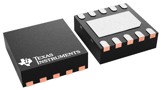
- 2.5 × 2.5 × 0.8 mm SON Package
Description for the TPS61093-Q1
The TPS61093-Q1 is a 1.2-MHz, fixed-frequency boost converter designed for high integration and high reliability. The IC integrates a 20-V power switch, input/output isolation switch, and power diode. When the output current exceeds the overload limit, the isolation switch of the IC opens up to disconnect the output from the input. This disconnection protects the IC and the input supply. The isolation switch also disconnects the output from the input during shut down to minimize leakage current. When the IC is shutdown, the output capacitor is discharged to a low voltage level by internal diodes. Other protection features include 1.1-A peak overcurrent protection (OCP) at each cycle, output overvoltage protection (OVP), thermal shutdown, and undervoltage lockout (UVLO).
With its 1.6-V minimum input voltage, the IC can be powered by two alkaline batteries, a single Li-ion battery, or 3.3-V and 5-V regulated supply. The output can be boosted up to 17-V. The TPS61093-Q1 is available in 2.5 mm × 2.5 mm SON package with thermal pad.