Features for the TSW3085EVM
Description for the TSW3085EVM
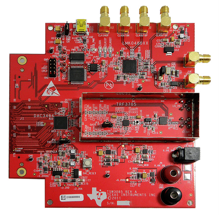
The TSW3085 Evalutaion Module is a circuit board that allows system designers to evaluate the combined performance of Texas Instruments' transmit signal chain with the LMK04806B (formally National Semiconductor) low noise clock generator/jitter cleaner. For ease of use as a complete RF transmit solution the TSW3085EVM includes the LMK04806B for clocking the DAC3482 digital-to-analog converter (DAC), as well as a TRF3705 for up-converting the I/Q output from the DACs to an RF carrier.
The DAC3482 is a dual-channel, ultra-low power 16-bit 1.25 GSPS DAC.
The TRF3705 is a high performance complex RF modulator with a 300 MHz to 4 GHz output range.
The LMK04806B is a low noise clock generator and jitter cleaner capable of jitter below 100fs rms and output frequencies up to 1300MHz.
The EVM can be used along with the TSW3100 pattern generator to perform a wide range of test procedures. The TSW3100 generates the test patterns which are fed to the DAC3482 through a 1.25 GSPS LVDS port. The LMK04806B is used to synchronize the TSW3100 board to the TSW3085EVM. The transmit RF signal path also includes an amplifier and programmable attenuator.