Packaging information
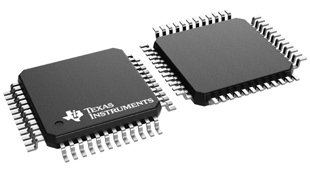
| Package | Pins TQFP (PFB) | 48 |
| Operating temperature range (°C) -40 to 85 |
| Package qty | Carrier 1,000 | LARGE T&R |
Features for the TWL1200-Q1
- Qualified for Automotive Applications
- AEC-Q100 Test Guidance With the Following Results:
- Device Temperature Grade 3: –40°C to +85°C
Ambient Operating Temperature Range - Device HBM ESD Classification Level H1C
- Device CDM ESD Classification Level C3B
- Device Temperature Grade 3: –40°C to +85°C
- Level Translator
- VCCA and VCCB Range of 1.1 V to 3.6 V
- Seamlessly Bridges 1.8-V/2.6-V Digital-Switching Compatibility Gap
Between 2.6-V processors and TI’s Wi-Link (WL1271 and WL1273) - Latch-Up Performance Exceeds 100 mA per JESD 78, Class II
Description for the TWL1200-Q1
The TWL1200-Q1 is a 19-bit voltage translator specifically designed to bridge seamlessly the 1.8-V/2.6-V digital-switching compatibility gap between 2.6-V baseband and the TI Wi-Link-6 (WL1271/3). The device is optimized for SDIO, UART, and audio functions. The TWL1200-Q1 has two supply-voltage pins, VCCA and VCCB, that can be operated over the full range of 1.1 V to 3.6 V. The TWL1200-Q1 enables system designers easily to interface applications processors or digital basebands to peripherals operating at a different I/O voltage levels, such as the TI Wi-Link-6 (WL1271/3) or other SDIO/memory cards.
The TWL1200-Q1 is offered in a thin quad flat pack [TQFP (PFB)] package. Low static power consumption and small package size make the TWL1200-Q1 an ideal choice for mobile-phone applications.