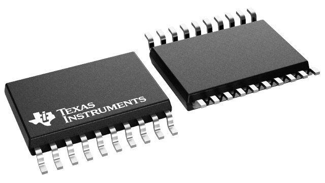
Packaging information
| Package | Pins TSSOP (PW) | 20 |
| Operating temperature range (°C) -40 to 85 |
| Package qty | Carrier 2,000 | LARGE T&R |
Features for the TXS0108E
- No Direction-Control Signal Needed
- Maximum Data Rates
- 110 Mbps (Push Pull)
- 1.2 Mbps (Open Drain)
- 1.4 V to 3.6 V on A Port and 1.65 V to 5.5 V on B Port (V CCA ≤ V CCB)
- No Power-Supply Sequencing Required – Either V CCA or V CCB Can Be Ramped First
- Latch-Up Performance Exceeds 100 mA Per JESD 78, Class II
- ESD Protection Exceeds JESD 22 (A Port)
- 2000 V Human Body Model (A114-B)
- 150 V Machine Model (A115-A)
- 1000 V Charged-Device Model (C101)
- IEC 61000-4-2 ESD (B Port)
- ±8 kV Contact Discharge
- ±6 kV Air-Gap Discharge
Description for the TXS0108E
This device is a 8-bit non-inverting level translator which uses two separate configurable power-supply rails. The A port tracks the V CCA pin supply voltage. The V CCA pin accepts any supply voltage between 1.4 V and 3.6 V. The B port tracks the V CCB pin supply voltage. The V CCB pin accepts any supply voltage between 1.65 V and 5.5 V. Two input supply pins allows for low Voltage bidirectional translation between any of the 1.5 V, 1.8 V, 2.5 V, 3.3 V, and 5 V voltage nodes.
When the output-enable (OE) input is low, all outputs are placed in the high-impedance (Hi-Z) state.
To ensure the Hi-Z state during power-up or power-down periods, tie OE to GND through a pull-down resistor. The minimum value of the resistor is determined by the current-sourcing capability of the driver.