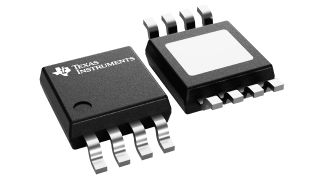
Packaging information
| Package | Pins HVSSOP (DGN) | 8 |
| Operating temperature range (°C) -40 to 140 |
| Package qty | Carrier 2,500 | LARGE T&R |
Features for the UCC27524A1-Q1
- Qualified for Automotive Applications
- AEC-Q100 Qualified With
the Following Results:
- Device Temperature Grade 1
- Device HBM ESD Classification Level H2
- Device CDM ESD Classification Level C4B
- Industry-Standard Pin Out
- Two Independent Gate-Drive Channels
- 5-A Peak Source and Sink-Drive Current
- Independent Enable Function for Each Output
- TTL and CMOS-Compatible Logic Threshold Independent of Supply Voltage
- Hysteretic-Logic Thresholds for High-Noise Immunity
- Ability to Handle Negative Voltages (–5 V) at Inputs
- Inputs and Enable Pin-Voltage Levels Not Restricted by VDD Pin Bias Supply Voltage
- 4.5-V to 18-V Single-Supply Range
- Outputs Held Low During VDD-UVLO, (Ensures Glitch-Free Operation at Power-Up and Power-Down)
- Fast Propagation Delays (13-ns typical)
- Fast Rise and Fall Times (7-ns and 6-ns Typical)
- 1-ns Typical Delay Matching Between 2-Channels
- Ability to Parallel Two Outputs for High-Drive Current
- Outputs Held in LOW When Inputs are Floating
- MSOP-8 PowerPad™ Package
- Operating Temperature Range of –40°C to +140°C
Description for the UCC27524A1-Q1
The UCC27524A1-Q1 device is a dual-channel, high-speed, low-side, gate-driver device capable of effectively driving MOSFET and IGBT power switches. The UCC27524A1-Q1 device is a variant of the UCC2752x family. The UCC27524A1-Q1 device adds the ability to handle –5 V directly at the input pins for increased robustness. The UCC27524A1-Q1 device is a dual, non-inverting driver. Using a design that inherently minimizes shoot-through current, the UCC27524A1-Q1 device is capable of delivering high-peak current pulses of up to 5-A source and 5-A sink into capacitive loads along with rail-to-rail drive capability and extremely small propagation delay (typically 13 ns). In addition, the drivers feature matched, internal-propagation delays between the two channels which are very well suited for applications requiring dual-gate drives with critical timing, such as synchronous rectifiers. This also enables connecting two channels in parallel to effectively increase current-drive capability or driving two switches in parallel with a single input signal. The input pin thresholds are based on TTL and CMOS compatible low-voltage logic, which is fixed and independent of the VDD supply voltage. Wide hysteresis between the high and low thresholds offers excellent noise immunity.
For protection purposes, internal pull-up and pull-down resistors on the input pins of the UCC27524A1-Q1 device ensure that outputs are held LOW when input pins are in floating condition. The UCC27524A1-Q1 device features enable pins (ENA and ENB) to have better control of the operation of the driver applications. The pins are internally pulled up to VDD for active-high logic and are left open for standard operation.
The UCC27524A1-Q1 devices is available in a MSOP-PowerPAD-8 with exposed pad (DGN) package.