AFE7769-3P5EVM 的特性
- Evaluates AFE77xx integrated transceiver family of devices
- Simplified digital interface with JESD204B/C; supports up to 29.5-Gbps lane rates
- JESD subclass 1 for multiple-device synchronization
- Onboard clocking solution with optional external feed
- Onboard power-management scheme
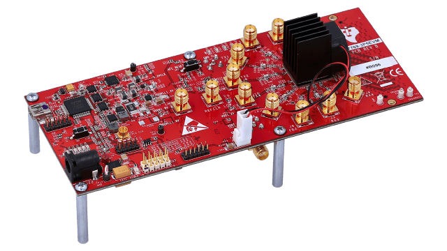
AFE7769-3P5EVM 的说明
The AFE7769-3P5 evaluation module (EVM) is a board used to evaluate the AFE77xx family of integrated RF transceivers. AFE7769 and AFE7799 devices support up to four-transmit, four-receive, and two feedback channels (4T4R2F) and integrate phase-locked loops (PLLs) and voltage-controlled oscillators (VCOs) for generation of data-converter clocks and LO, with LO frequency tunable from 600 MHz to 6 GHz.
AFE7769-3P5EVM incorporates radio-frequency (RF) baluns and matching to specifically support 3.3 GHz to 3.8 GHz, but can be extended to support up to 6 GHz. AFE77xx devices integrate eight JESD204B/C-compatible serializer/deserializer (SerDes) transceivers capable of running up to 29.5 Gbps to transmit and receive digital data through the onboard FPGA mezzanine card (FMC) connector.
AFE7769-3P5EVM includes the LMK04828 clock generator for providing reference clocks and sysref to the analog front end (AFE) and capture card (FPGA). The EVM works off a single 6-V input and includes complete power management. External clocking options include support for feeding the reference clock (for on-chip PLL) or the channel frequency (at 2× LO).
The design interfaces with the TI pattern/capture card solutions (TSW14J56EVM and TSW14J57EVM, sold separately), as well as many FPGA development kits.