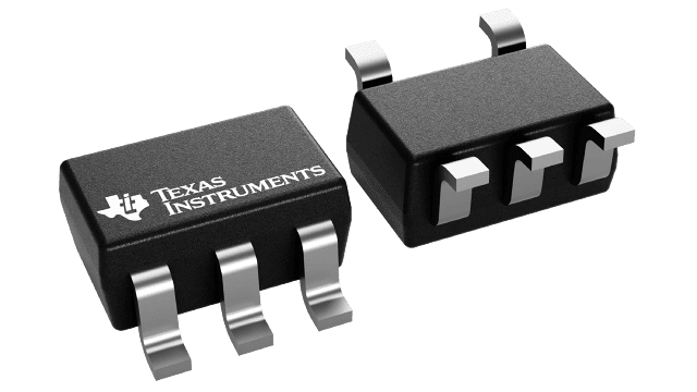
封装信息
| 封装 | 引脚 SOT-SC70 (DCK) | 5 |
| 工作温度范围 (°C) -40 to 85 |
| 包装数量 | 包装 3,000 | LARGE T&R |
SN74AUP1G126 的特性
- Latch-Up Performance Exceeds 100 mA Per JESD 78, Class II
- ESD Performance Tested Per JESD 22−
- 2000-V Human-Body Model
(A114-B, Class II) - 1000-V Charged-Device Model (C101)
- 2000-V Human-Body Model
- Available in the Texas Instruments NanoStar™ Package
- Low Static-Power Consumption
(ICC = 0.9 µA Maximum) - Low Dynamic-Power Consumption
(Cpd = 4 pF Typical at 3.3 V) - Low Input Capacitance (Ci = 1.5 pF Typical)
- Low Noise – Overshoot and Undershoot
<10% of VCC - Input-Disable Feature Allows Floating Input Conditions
- Ioff Supports Partial-Power-Down Mode Operation
- Input Hysteresis Allows Slow Input Transition and Better Switching Noise Immunity at Input
- Wide Operating VCC Range of 0.8 V to 3.6 V
- Optimized for 3.3-V Operation
- 3.6-V I/O Tolerant to Support Mixed-Mode Signal Operation
- tpd = 4.6 ns Maximum at 3.3 V
- Suitable for Point-to-Point Applications
SN74AUP1G126 的说明
The AUP family is TI’s premier solution to the industry’s low-power needs in battery-powered portable applications. This family assures a very low static and dynamic power consumption across the entire VCC range of 0.8 V to 3.6 V, resulting in an increased battery life. This product also maintains excellent signal integrity (see AUP – The Lowest-Power Family and Excellent Signal Integrity ).
This bus buffer gate is a single line driver with a 3-state output. The output is disabled when the output-enable (OE) input is low. This device has the input-disable feature, which allows floating input signals.
To assure the high-impedance state during power up or power down, OE should be tied to GND through a pulldown resistor; the minimum value of the resistor is determined by the current-sourcing capability of the driver.
NanoStar™ package technology is a major breakthrough in IC packaging concepts, using the die as the package.
This device is fully specified for partial-power-down applications using Ioff. The Ioff circuitry disables the outputs when the device is powered down. This inhibits current backflow into the device which prevents damage to the device.
